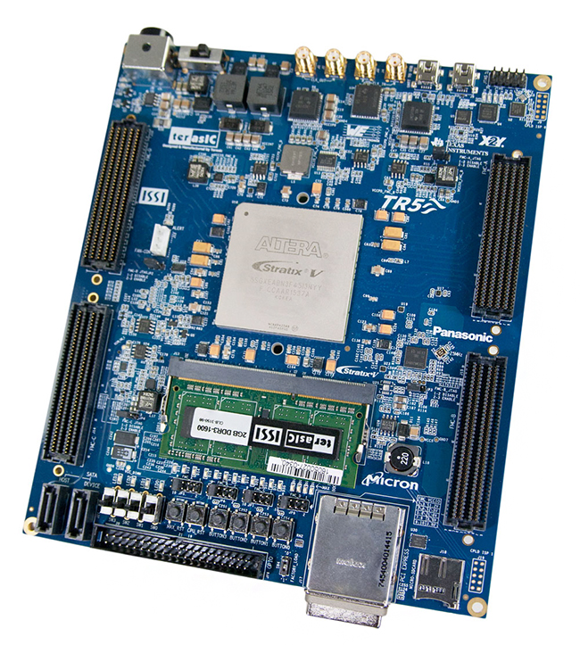
 TR5 FPGA development kit using the Altera Stratix V GX FPGA provides high-speed operation and transmission with large capacity up to 622K LE.
The board provides four FMC connectors and a 2x20 GPIO connector. It offers a total of more than 500 I/Os for users to expand the usage with the peripherals connected. There are built-in high-speed DDR3 memory and SSRAM to increase the bandwidth for accessing large amounts of data for high-speed computation. In addition, the board also has PCIe andSATA interfaces for high-speed data transmission.

Four FMC connectors

2x20 GPIO connector
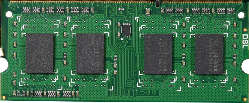
DDR3 memory
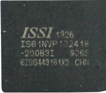
SSRAM
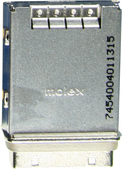
PCIe
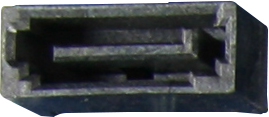
SATA
The main applications of TR5 are ASIC prototyping validation and the establishment of prototype systems. The FMC connectors onboard are standard interfaces. Users can purchase or develop various FMC daughter cards to expand their system. For developers who need to use multiple FPGAs, they can leverage Terasic’s FMC or PCIe cable to establish an inter-stackable multi-boards communication system. Users can also purchase Terasic PCIe daughter card to communicate with host PC.
 The TR5 development kit includes a variety of reference design examples for peripherals such as DDR3 SDRAM, SD card, USB-to-UART, SATA, PCIe, and an FMC connector. The kit is user friendly and enables users to quickly get started or verify the functions. The kit also provides a tool named "System Builder" software. It can automatically generate a complete Quartus project including pin assignment and clock configuration IP upon users selections of peripherals, FMC daughter cards, and a designated clock frequency. It helps users avoid time-consuming and error-prone manual pin-assignment work.

