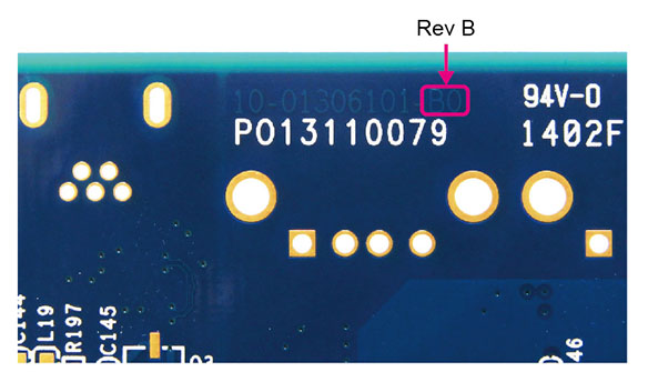
How to distinguish rev. B~ rev. H board?
As shown in the figure below, if the letter inside the red circle is "B0", it means that the PCB version is Rev.B.
"H0"means that the PCB version is Rev.H
What are the parts changed?
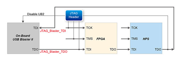
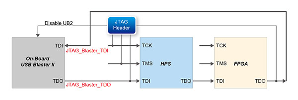
The JTAG chain has been changed. Starting from rev. C, the HPS comes before FPGA in the JTAG chain.
This is to bypass a bug in the DS-5 where reset can't function properly.
The difference between DE1-SoC rev. C and rev. D:
Both 5V and GPIO 3.3V power are provided by two different power module LTM4624 respectively in rev. C. In rev. D, 5V power is provided by one LTC3605 regulator instead of LTC4624, GPIO 3.3V power is provided by one original on-board LTC3605 regulator which provides all 3.3V power for DE1-SoC board.
rev. B JTAG chain: USB Blaster II ---> FPGA ---> HPS ---> USB Blaster II
JTAG chain starting from rev. C: USB Blaster II ---> HPS ---> FPGA ---> USB Blaster II
The difference between DE1-SoC rev. D and rev. E:
The serial configuration device has been changed from EPCQ256 to EPCS128.
The difference between DE1-SoC rev. E and rev. F:
The analog-to-digital (ADC) chip has been changed from AD7928 to LTC2308.
The difference between DE1-SoC rev. F and rev. G:
Remove Logo of the "Linear " and "MICROCHIP " on the rev. F PCB.
The difference between DE1-SoC rev. G and rev. H:
DE1-SoC Rev.G to Rev.H Revision List
Changes in the CD-ROM
| Item | Description |
|---|---|
| Schematic | JTAG Chain |
| User Manual | Modified Figures involving Quartus Programming and JTAG description |
| Demonstration Code | Batch file can automatically detect FPGA device index such that the code can be used for both revision boards. |