PCA3 User Manual
From Terasic Wiki
(→LEDs) |
(→LEDs) |
||
| (29 intermediate revisions not shown) | |||
| Line 1: | Line 1: | ||
=Chapter 1 Introduction= | =Chapter 1 Introduction= | ||
| - | + | PCA3 (PCIe Cable Adapter, Gen 3) is a conversion card to connect boards with your host PC. It can support up to PCIe Gen 3 x4. Users with boards such as Terasic TR4 and TR5 can establish high-speed data transmission through this card and the PCIe cable via PCIe connector to any host PC. It provides automatic rate-detect and adaptation to PCIe Gen-1, Gen-2 and Gen-3 speeds. | |
==Features== | ==Features== | ||
Figure 1-1 shows a photograph of the PCA3 card.<br/> | Figure 1-1 shows a photograph of the PCA3 card.<br/> | ||
| - | + | :::[[File:PCA3 Exterior View.jpg|350px]]<br/> | |
| - | + | ::::::Figure 1-1 Exterior View<br/> | |
The key features of the card are listed below:<br/> | The key features of the card are listed below:<br/> | ||
:*Up to 8.0Gbps PCIe 3.0 Serial Re-Driver | :*Up to 8.0Gbps PCIe 3.0 Serial Re-Driver | ||
| Line 31: | Line 31: | ||
==Block Diagram of the PCA3 Board== | ==Block Diagram of the PCA3 Board== | ||
Figure 2-3 shows the block diagram of the PCA3 card.<br/> | Figure 2-3 shows the block diagram of the PCA3 card.<br/> | ||
| - | :::[[File: | + | :::[[File:PCA3 block diagram.png|600px]]<br/> |
:::::::::Figure 2-3 Block Diagram of PCA3 | :::::::::Figure 2-3 Block Diagram of PCA3 | ||
| Line 39: | Line 39: | ||
==PCIe Edge Connector== | ==PCIe Edge Connector== | ||
This PCIe edge connector is used to connect the PCA3 with PC motherboard PCIe slot, as show Figure 3-1 and Figure 3-2.<br/><br/> | This PCIe edge connector is used to connect the PCA3 with PC motherboard PCIe slot, as show Figure 3-1 and Figure 3-2.<br/><br/> | ||
| - | ::[[File: | + | :::[[File:Pca3.png|500px]]<br/> |
| - | ::::::Figure 3-1 PCA3 Edge Connector<br/><br/> | + | :::::::::Figure 3-1 PCA3 Edge Connector<br/><br/><br/> |
| - | ::[[File: | + | :::[[File:PCa3 connection.png|550px]]<br/> |
| - | :::::Figure 3-2 Plug the PCA3 into the PCIe slot of the Motherboard<br/> | + | ::::::::Figure 3-2 Plug the PCA3 into the PCIe slot of the Motherboard<br/> |
The pins are numbered as shown in Table 3-1 with side A on the top of the center-line on the solder side of the board and side B on the bottom of the centerline on the component side of the board.<br/> | The pins are numbered as shown in Table 3-1 with side A on the top of the center-line on the solder side of the board and side B on the bottom of the centerline on the component side of the board.<br/> | ||
| - | The PCIe interface pins PETpx, PETnx, PERpx, and PERnx are named with the following convention: | + | The PCIe interface pins PETpx, PETnx, PERpx, and PERnx are named with the following convention:"PE" stands for PCIe high speed,"T" for Transmitter,"R" for Receiver,"p" for positive (+), and "n" for negative (-).<br/> |
| - | Note that adjacent differential pairs are separated by two ground pins to manage the connector crosstalk. | + | Note that adjacent differential pairs are separated by two ground pins to manage the connector crosstalk.Table 3-1 gives the wiring information of the PCIe Edge connector.<br/> |
| - | Table 3-1 gives the wiring information of the PCIe Edge connector.<br/> | + | |
::Table 3-1 Pin assignments and descriptions on PCIe Edge connector | ::Table 3-1 Pin assignments and descriptions on PCIe Edge connector | ||
:{| class="wikitable" | :{| class="wikitable" | ||
| Line 122: | Line 121: | ||
|32 ||GND||Ground||RSVD||Reserved | |32 ||GND||Ground||RSVD||Reserved | ||
|} | |} | ||
| - | |||
==PCIe Cable Connector== | ==PCIe Cable Connector== | ||
A PCIe cable connector is used to connect the PCIe x4 Cable and PCA cable connector, connect the adapter by using a PCIe x4 Cable, as show Figure 3-3.<br/> | A PCIe cable connector is used to connect the PCIe x4 Cable and PCA cable connector, connect the adapter by using a PCIe x4 Cable, as show Figure 3-3.<br/> | ||
| - | ::[[File:PCIe x4 Cable and PCA3.jpg|500px]]<br/> | + | :::[[File:PCIe x4 Cable and PCA3.jpg|500px]]<br/> |
:::::::Figure 3-3 PCIe x4 Cable and PCA3<br/><br/> | :::::::Figure 3-3 PCIe x4 Cable and PCA3<br/><br/> | ||
| - | To purchase the PCIe x4 Cable, please refer to the url: | + | To purchase the PCIe x4 Cable, please refer to the url: [http://www.terasic.com.tw/cgi-bin/page/archive.pl?Language=English&CategoryNo=77&No=687 PCIe x4 Gen.2 Cable]<br/><br/> |
Figure 3-4 shows the PCIe Cable connects PCA3 connector.<br/> | Figure 3-4 shows the PCIe Cable connects PCA3 connector.<br/> | ||
| - | ::[[File: | + | :::[[File:Cable connection.png|500px]]<br/> |
:::::Figure 3-4 PCIe Cable and PCA3 connector Connected<br/> | :::::Figure 3-4 PCIe Cable and PCA3 connector Connected<br/> | ||
Table 3-2 gives the wiring information of the PCIe Cable connector.<br/> | Table 3-2 gives the wiring information of the PCIe Cable connector.<br/> | ||
| Line 174: | Line 172: | ||
|A18 ||CPRSNTn ||Used for detection of whether a cable is installed and the downstream subsystem is powered | |A18 ||CPRSNTn ||Used for detection of whether a cable is installed and the downstream subsystem is powered | ||
|- | |- | ||
| - | |A19 ||CPWRON ||Turns power on / off to slave type downstream subsystems | + | |A19 ||CPWRON ||Turns power on/off to slave type downstream subsystems |
|- | |- | ||
|B1 ||GND ||Ground reference for PCI Express transmitter Lanes | |B1 ||GND ||Ground reference for PCI Express transmitter Lanes | ||
| Line 202: | Line 200: | ||
|B13 ||GND ||Ground reference for PCI Express transmitter Lanes | |B13 ||GND ||Ground reference for PCI Express transmitter Lanes | ||
|- | |- | ||
| - | |B14 ||PWR ||+3. | + | |B14 ||PWR ||+3.3V Cable power |
|- | |- | ||
| - | |B15 ||PWR ||+3. | + | |B15 ||PWR ||+3.3V Cable power |
|- | |- | ||
|B16 ||PWR RTN ||Cable power return | |B16 ||PWR RTN ||Cable power return | ||
| Line 214: | Line 212: | ||
|B19 ||CPERSTn ||Cable PERSTn | |B19 ||CPERSTn ||Cable PERSTn | ||
|} | |} | ||
| - | |||
==LEDs== | ==LEDs== | ||
The PCA3 includes status LEDs, please refer to Table 3-7 for the status of the LED indicator.<br/> | The PCA3 includes status LEDs, please refer to Table 3-7 for the status of the LED indicator.<br/> | ||
| - | + | :Table 3-7 Status of the LED indicator<br/> | |
:{| class="wikitable" | :{| class="wikitable" | ||
|- | |- | ||
| Line 228: | Line 225: | ||
|- | |- | ||
|D3 ||POWER ||Power LED | |D3 ||POWER ||Power LED | ||
| + | |} | ||
| + | |||
| + | ==Lane Re-driver IC== | ||
| + | A Lane Re-driver IC U1(DS80PCI402) is implemented on PCA3 board. In addition to supporting the 4-lane repeater function, DS80PCI402 chip also supports some modifiable parameters, such as input equalization, internal Signal Detect Threshold and loopback function. These functions can be set up by some of the resistances on PCA3 board, Figure 3-5 shows the resistances setting. Table 3-4 list pin configuration and function.<br/> | ||
| + | :::[[File:Resistance.jpg|600px]]<br/> | ||
| + | :::::::::Figure 3-5 Resistances setting<br/><br/> | ||
| + | |||
| + | :::::::::Table 3-4 Pin configuration and function | ||
| + | :{| class="wikitable" | ||
| + | |- | ||
| + | !Pin Numbers !!Name !!Description | ||
|- | |- | ||
| - | | | + | |19 ||EQA1 ||EQA1 control the level of equalization on the input pins. <br/>The pins are active only when ENSMB is deasserted (low). |
| + | |- | ||
| + | |20 ||EQA0 ||EQA0 control the level of equalization on the input pins. <br/>The pins are active only when ENSMB is deasserted (low). | ||
| + | |- | ||
| + | |21 ||RATE ||RATE control pin selects GEN 1,2 and GEN 3 operating modes.<br/>Tie 1kΩ to GND = GEN 1,2<br/>FLOAT = AUTO Rate Select of Gen1/2 and Gen3 with de-emphasis<br/>Tie 20kΩ to GND = GEN 3 without de-emphasis<br/>Tied 1kΩ to VDD = RESERVED | ||
| + | |- | ||
| + | |22 ||RXDET ||The RXDET pin controls the receiver detect function. <br/>Depending on the input level, a 50Ω or > 50kΩ termination to the power rail is enabled. | ||
| + | |- | ||
| + | |23 ||LPBK ||Controls the loopback function<br/>Tie 1kΩ to GND = Root Complex Loopback (INA_n to OUTB_n)<br/>Float = Normal Operation<br/>Tie 1kΩ to VDD = End-point Loopback (INB_n to OUTA_n) | ||
| + | |- | ||
| + | |26 ||SD_TH ||Controls the internal Signal Detect Threshold | ||
|} | |} | ||
| + | |||
| + | =Chapter 4 Setup= | ||
| + | |||
| + | =Chapter 5 Appendix= | ||
| + | ==Revision History== | ||
| + | :{| class="wikitable" | ||
| + | |- | ||
| + | !Version !!Change Log | ||
| + | |- | ||
| + | |V1.0 ||Initial Version (Preliminary) | ||
| + | |} | ||
| + | |||
| + | ==Copyright Statement== | ||
| + | :Copyright © 2012 Terasic Technologies. All rights reserved. | ||
Latest revision as of 17:44, 30 October 2017
Contents |
Chapter 1 Introduction
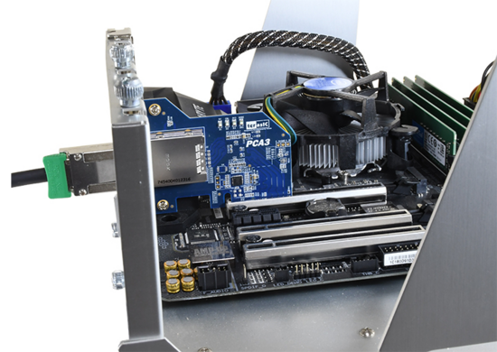
PCA3 (PCIe Cable Adapter, Gen 3) is a conversion card to connect boards with your host PC. It can support up to PCIe Gen 3 x4. Users with boards such as Terasic TR4 and TR5 can establish high-speed data transmission through this card and the PCIe cable via PCIe connector to any host PC. It provides automatic rate-detect and adaptation to PCIe Gen-1, Gen-2 and Gen-3 speeds.
Features
Figure 1-1 shows a photograph of the PCA3 card.
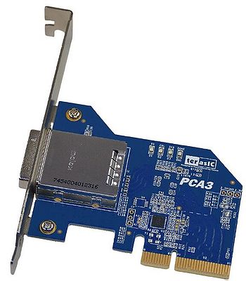
- Figure 1-1 Exterior View
- Figure 1-1 Exterior View

The key features of the card are listed below:
- Up to 8.0Gbps PCIe 3.0 Serial Re-Driver
- PCIe x4 Gen 3
- Adjustable receiver equalization
- Adjustable transmitter amplitude and de-emphasis
Getting Help
Here is information of how to get help if you encounter any problem:
Terasic Technologies
- Tel: +886-3-550-8800
- Email: support@terasic.com.cn
Chapter 2 Architecture
This chapter provides information about architecture and block diagram of the PCA3 board.
Layout and Components
The picture of the Terasic PCIe x4 Cable Adapter (PCA3) is shown in Figure 2-1 and Figure 2-2. It depicts the layout of the board and indicates the locations of the connectors and key components.
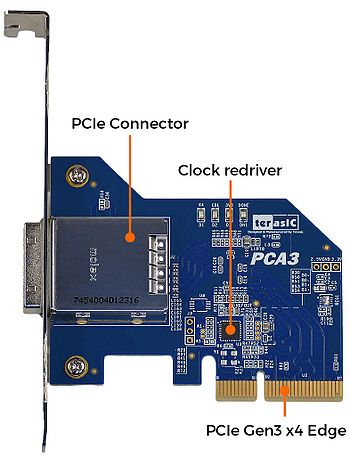
- Figure 2-1 The PCA3 Card PCB and Component Diagram (top view)

- Figure 2-2 The PCA3 Card PCB and Component Diagram (bottom view)

Block Diagram of the PCA3 Board
Figure 2-3 shows the block diagram of the PCA3 card.
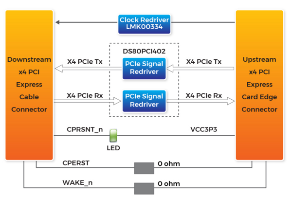
- Figure 2-3 Block Diagram of PCA3

Chapter 3 Board Components
This chapter describes the specifications of the onboard components.
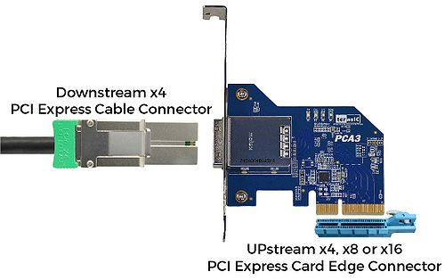
PCIe Edge Connector
This PCIe edge connector is used to connect the PCA3 with PC motherboard PCIe slot, as show Figure 3-1 and Figure 3-2.
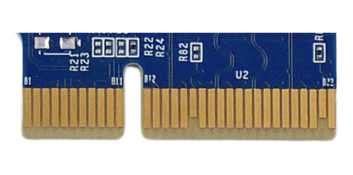
- Figure 3-1 PCA3 Edge Connector
- Figure 3-1 PCA3 Edge Connector

- Figure 3-2 Plug the PCA3 into the PCIe slot of the Motherboard
- Figure 3-2 Plug the PCA3 into the PCIe slot of the Motherboard

The pins are numbered as shown in Table 3-1 with side A on the top of the center-line on the solder side of the board and side B on the bottom of the centerline on the component side of the board.
The PCIe interface pins PETpx, PETnx, PERpx, and PERnx are named with the following convention:"PE" stands for PCIe high speed,"T" for Transmitter,"R" for Receiver,"p" for positive (+), and "n" for negative (-).
Note that adjacent differential pairs are separated by two ground pins to manage the connector crosstalk.Table 3-1 gives the wiring information of the PCIe Edge connector.
- Table 3-1 Pin assignments and descriptions on PCIe Edge connector
Pin Numbers Side B Side A Name Description Name Description 1 NC NC PRSNT1n Hot-Plug presence detect 2 NC NC NC NC 3 NC NC NC NC 4 GND Ground GND Ground 5 SMCLK System Clock NC NC 6 SMDAT System Data Line NC NC 7 GND Ground NC NC 8 VCC3P3 3.3V Power NC NC 9 NC NC VCC3P3 3.3V Power 10 3.3VAUX 3.3V Auxiliary Power VCC3P3 3.3V Power 11 WAKE NC PERSTn Fundamental Reset Mechanical Key 12 RSVD Reserved GND Ground 13 GND Ground REFCLK+ Reference clock
(differential pair)14 PETp0 Transmitter differential
pair,Lane 0REFCLK- 15 PETn0 GND Ground 16 GND Ground PERp0 Receiver differential
pair, Lane 017 PRSNT2n Hot-Plug presence detect PERn0 18 GND Ground GND Ground 19 PETp1 Transmitter differential
pair,Lane 1RSVD Reserved 20 PETn1 GND Ground 21 GND Ground PERp1 Receiver differential
pair, Lane 122 GND Ground PERn1 23 PETp2 Transmitter differential
pair,Lane 2GND Ground 24 PETn2 GND Ground 25 GND Ground PERp2 Receiver differential
pair, Lane 226 GND Ground PERn2 27 PETp3 Transmitter differential
pair,Lane 3GND Ground 28 PETn3 GND Ground 29 GND Ground PERp3 Receiver differential
pair, Lane 330 RSVD Reserved PERn3 31 PRSNT2n Hot-Plug presence detect GND Ground 32 GND Ground RSVD Reserved
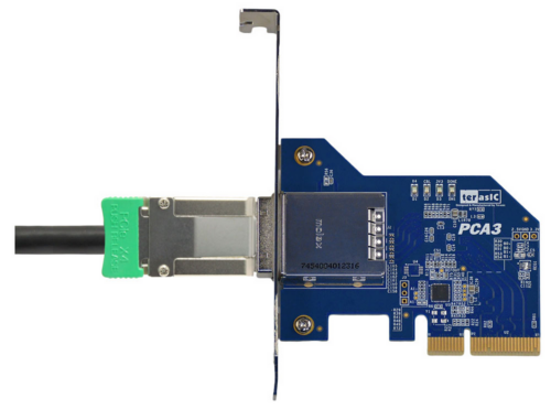
PCIe Cable Connector
A PCIe cable connector is used to connect the PCIe x4 Cable and PCA cable connector, connect the adapter by using a PCIe x4 Cable, as show Figure 3-3.
- Figure 3-3 PCIe x4 Cable and PCA3
- Figure 3-3 PCIe x4 Cable and PCA3

To purchase the PCIe x4 Cable, please refer to the url: PCIe x4 Gen.2 Cable
Figure 3-4 shows the PCIe Cable connects PCA3 connector.
- Figure 3-4 PCIe Cable and PCA3 connector Connected
- Figure 3-4 PCIe Cable and PCA3 connector Connected

Table 3-2 gives the wiring information of the PCIe Cable connector.
- Table 3-2 Wiring information of the PCIe Cable connector
- Table 3-2 Wiring information of the PCIe Cable connector
Pin Numbers Name Description A1 GND Ground reference for PCI Express transmitter Lanes A2 PETp0 Differential PCI Express transmitter Lane 0 A3 PETn0 Differential PCI Express transmitter Lane 0 A4 GND Ground reference for PCI Express transmitter Lanes A5 PETp1 Differential PCI Express transmitter Lane 1 A6 PETn1 Differential PCI Express transmitter Lane 1 A7 GND Ground reference for PCI Express transmitter Lanes A8 PETp2 Differential PCI Express transmitter Lane 2 A9 PETn2 Differential PCI Express transmitter Lane 2 A10 GND Ground reference for PCI Express transmitter Lanes A11 PETp3 Differential PCI Express transmitter Lane 3 A12 PETn3 Differential PCI Express transmitter Lane 3 A13 GND Ground reference for PCI Express transmitter Lanes A14 CREFCLK+ Differential 100MHz cable reference clock A15 CREFCLK- Differential 100MHz cable reference clock A16 GND Ground reference for PCI Express transmitter Lanes A17 SB_RTN Signal return for single ended sideband signals A18 CPRSNTn Used for detection of whether a cable is installed and the downstream subsystem is powered A19 CPWRON Turns power on/off to slave type downstream subsystems B1 GND Ground reference for PCI Express transmitter Lanes B2 PERp0 Differential PCI Express receiver Lane 0 B3 PERn0 Differential PCI Express receiver Lane 0 B4 GND Ground reference for PCI Express transmitter Lanes B5 PERp1 Differential PCI Express receiver Lane 1 B6 PERn1 Differential PCI Express receiver Lane 1 B7 GND Ground reference for PCI Express transmitter Lanes B8 PERp2 Differential PCI Express receiver Lane 2 B9 PERn2 Differential PCI Express receiver Lane 2 B10 GND Ground reference for PCI Express transmitter Lanes B11 PERp3 Differential PCI Express receiver Lane 3 B12 PERn3 Differential PCI Express receiver Lane 3 B13 GND Ground reference for PCI Express transmitter Lanes B14 PWR +3.3V Cable power B15 PWR +3.3V Cable power B16 PWR RTN Cable power return B17 PWR RTN Cable power return B18 CWAKEn Power management signal for wakeup events (optional) B19 CPERSTn Cable PERSTn
LEDs
The PCA3 includes status LEDs, please refer to Table 3-7 for the status of the LED indicator.
- Table 3-7 Status of the LED indicator
Board Reference LED name Description D1 CBL Cable PRSNT1n D2 EDGE Edge PRSNT1n D3 POWER Power LED
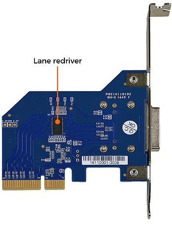
Lane Re-driver IC
A Lane Re-driver IC U1(DS80PCI402) is implemented on PCA3 board. In addition to supporting the 4-lane repeater function, DS80PCI402 chip also supports some modifiable parameters, such as input equalization, internal Signal Detect Threshold and loopback function. These functions can be set up by some of the resistances on PCA3 board, Figure 3-5 shows the resistances setting. Table 3-4 list pin configuration and function.
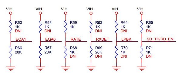
- Figure 3-5 Resistances setting
- Figure 3-5 Resistances setting

- Table 3-4 Pin configuration and function
Pin Numbers Name Description 19 EQA1 EQA1 control the level of equalization on the input pins.
The pins are active only when ENSMB is deasserted (low).20 EQA0 EQA0 control the level of equalization on the input pins.
The pins are active only when ENSMB is deasserted (low).21 RATE RATE control pin selects GEN 1,2 and GEN 3 operating modes.
Tie 1kΩ to GND = GEN 1,2
FLOAT = AUTO Rate Select of Gen1/2 and Gen3 with de-emphasis
Tie 20kΩ to GND = GEN 3 without de-emphasis
Tied 1kΩ to VDD = RESERVED22 RXDET The RXDET pin controls the receiver detect function.
Depending on the input level, a 50Ω or > 50kΩ termination to the power rail is enabled.23 LPBK Controls the loopback function
Tie 1kΩ to GND = Root Complex Loopback (INA_n to OUTB_n)
Float = Normal Operation
Tie 1kΩ to VDD = End-point Loopback (INB_n to OUTA_n)26 SD_TH Controls the internal Signal Detect Threshold
Chapter 4 Setup
Chapter 5 Appendix
Revision History
Version Change Log V1.0 Initial Version (Preliminary)
Copyright Statement
- Copyright © 2012 Terasic Technologies. All rights reserved.