DE10-Pro Board Revision Document
From Terasic Wiki
(→Product Roadmap) |
|||
| Line 83: | Line 83: | ||
{|style="border-spacing:0;width:14.651cm;" | {|style="border-spacing:0;width:14.651cm;" | ||
|- | |- | ||
| - | | style="background-color:#bfbfbf;border-top:0.5pt solid #000000;border-bottom:0.5pt solid #000000;border-left:0.5pt solid #000000;border-right:none;padding-top:0cm;padding-bottom:0cm;padding-left:0.191cm;padding-right:0.191cm;color:#000000;" | '''Revision''' | + | | style="background-color:#bfbfbf;border-top:0.5pt solid #000000;border-bottom:0.5pt solid #000000;border-left:0.5pt solid #000000;border-right:none;padding-top:0cm;padding-bottom:0cm;padding-left:0.191cm;padding-right:0.191cm;color:#000000;" | '''PCB Revision''' |
| style="background-color:#bfbfbf;border:0.5pt solid #000000;padding-top:0cm;padding-bottom:0cm;padding-left:0.191cm;padding-right:0.191cm;color:#000000;" | '''Description''' | | style="background-color:#bfbfbf;border:0.5pt solid #000000;padding-top:0cm;padding-bottom:0cm;padding-left:0.191cm;padding-right:0.191cm;color:#000000;" | '''Description''' | ||
|- | |- | ||
| Line 90: | Line 90: | ||
|- | |- | ||
| style="border-top:0.5pt solid #000000;border-bottom:0.5pt solid #000000;border-left:0.5pt solid #000000;border-right:none;padding-top:0cm;padding-bottom:0cm;padding-left:0.191cm;padding-right:0.191cm;color:#000000;" | D | | style="border-top:0.5pt solid #000000;border-bottom:0.5pt solid #000000;border-left:0.5pt solid #000000;border-right:none;padding-top:0cm;padding-bottom:0cm;padding-left:0.191cm;padding-right:0.191cm;color:#000000;" | D | ||
| - | | style="border:0.5pt solid #000000;padding-top:0cm;padding-bottom:0cm;padding-left:0.191cm;padding-right:0.191cm;color:#000000;" | 1. Modify HPS LED circuit to fix HPS LED brightness issue: | + | | style="border:0.5pt solid #000000;padding-top:0cm;padding-bottom:0cm;padding-left:0.191cm;padding-right:0.191cm;color:#000000;" | |
| + | 1.Modify HPS LED circuit to fix HPS LED brightness issue: | ||
| + | |||
GX: 1SG280HU1F50E1VG | GX: 1SG280HU1F50E1VG | ||
| + | |||
SX: 1SX280HU2F50E1VG | SX: 1SX280HU2F50E1VG | ||
| - | The SX FPGA DE10-Pro board has a MicroSD card socket, EPCQ device | + | |
| - | and HPS daughter card connector while the GX FPGA DE10-Pro board | + | The SX FPGA DE10-Pro board has a MicroSD card socket, EPCQ device and HPS daughter card connector while the GX FPGA DE10-Pro board hasn’t. |
| - | hasn’t. | + | |
| + | 2. Due to FPGA device is -1 core speed, DDR4 SODIMM module is replaced with DDR4-2666 DDR4 module. | ||
| + | |||
| + | 3. Modify HPS LED circuit to fix HPS LED brightness issue. | ||
| + | |- | ||
| + | | style="border-top:0.5pt solid #000000;border-bottom:0.5pt solid #000000;border-left:0.5pt solid #000000;border-right:none;padding-top:0cm;padding-bottom:0cm;padding-left:0.191cm;padding-right:0.191cm;color:#000000;" | E | ||
| + | | style="border:0.5pt solid #000000;padding-top:0cm;padding-bottom:0cm;padding-left:0.191cm;padding-right:0.191cm;color:#000000;" | | ||
| + | 1. Change FPGA device to only support SX: 1SX280HU2F50E1VG. | ||
| + | |||
| + | 2. Add clock mux/buffer Si53307-B-GM and SW7 to ensure DDR4A port can fully support DDR4 reference clock requirements of FPGA DDR4 and HPS DDR4. | ||
| + | |||
|- | |- | ||
|} | |} | ||
Revision as of 10:16, 20 June 2020
Contents |
Product Roadmap
The figure below shows the DE10-Pro product name corresponds to PCB version.
The detailed FPGA sepcifiaction of each product name are list in the table below:
| Item | PCB Version | Product Number | Product Name | Family Part Number | Family Variant | Logic Density |
| 1 | B | P0576 | DE10-Pro-GL2E1 | 1SG280LU2F50E1VG | GX | 2800K |
| 2 | C | P0536/P0612 | DE10-Pro-GH2E2-280 | 1SG280HU2F50E2VG | GX | 2800K |
| 3 | C | P0592/P0613 | DE10-Pro-GH2E2-165 | 1SG165HU2F50E2VG | GX | 1650K |
| 4 | C | P0620 | DE10-Pro-SL2E1-280 | 1SX280LU2F50E1VG | SX | 2800K |
| 5 | D | P0626/P0628 | DE10-Pro-GX-280 | 1SG280HU1F50E1VG | GX | 2800K |
| 6 | D | P0627/P0629 | DE10-Pro-SX-280 | 1SX280HU2F50E1VG | SX | 2800K |
| 7 | E | P0627/P0629 | DE10-Pro-SX-280 | 1SX280HU2F50E1VG | SX | 2800K |
Board Revision Details
| PCB Revision | Description |
| C | Released |
| D |
1.Modify HPS LED circuit to fix HPS LED brightness issue: GX: 1SG280HU1F50E1VG SX: 1SX280HU2F50E1VG The SX FPGA DE10-Pro board has a MicroSD card socket, EPCQ device and HPS daughter card connector while the GX FPGA DE10-Pro board hasn’t. 2. Due to FPGA device is -1 core speed, DDR4 SODIMM module is replaced with DDR4-2666 DDR4 module. 3. Modify HPS LED circuit to fix HPS LED brightness issue. |
| E |
1. Change FPGA device to only support SX: 1SX280HU2F50E1VG. 2. Add clock mux/buffer Si53307-B-GM and SW7 to ensure DDR4A port can fully support DDR4 reference clock requirements of FPGA DDR4 and HPS DDR4. |
How to Find the DE10-Pro Board Revision?
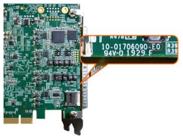
On the bottom view of the PCB, there is a seal mark for the board hardware version.
As shown in the figure below, if the letter inside the red circle is "E", it means that the PCB version is Rev.E.
What's Differences between the DE10-Pro SX and DE10-Pro GX
The difference between DE10-Pro GX and DE10-Pro SX is the FPGA device part number of the Stratix 10 FPGA on the board. The DE10-Pro SX's FPGA usning SoC FPGA built-in Quad-core ARM * Cortex * -A53 MPCore * processor and other peripheral controllers.
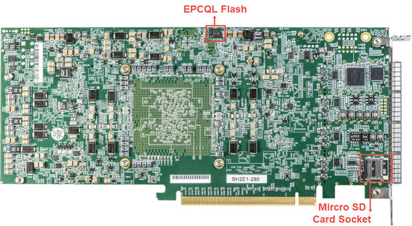
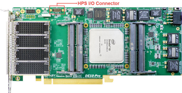
The DE10-Pro SX and DE10-Pro GX products use the same PCB, but the DE10_Pro SX will have the following three interfaces in particular:
- Micro SD Card Socket for HPS booting
- HPS I/O Connector for connecting expansion HPS interface Card
- EPCQL flash for booting
These components are not included in the DE10-Pro GX version.


