DE10-Advanced User Manual
From Terasic Wiki
(→SATA) |
(→PCIe) |
||
| Line 394: | Line 394: | ||
The PCI Express interface supports complete PCI Express Gen1 at 2.5Gbps/lane, Gen2 at 5.0Gbps/lane, and Gen3 at 8.0Gbps/lane protocol stack solution compliant to PCI Express base specification 3.0 that includes PHY-MAC, Data Link, and transaction layer circuitry embedded in PCI Express hard IP blocks. | The PCI Express interface supports complete PCI Express Gen1 at 2.5Gbps/lane, Gen2 at 5.0Gbps/lane, and Gen3 at 8.0Gbps/lane protocol stack solution compliant to PCI Express base specification 3.0 that includes PHY-MAC, Data Link, and transaction layer circuitry embedded in PCI Express hard IP blocks. | ||
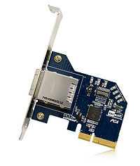
| - | To use PCIe interface, two external associated devices will be needed to establish a link with PC. First, a PCIe half-height add-in host card with a PCIe x4 cable connector called PCA (PCIe Cabling Adapter Card and see | + | To use PCIe interface, two external associated devices will be needed to establish a link with PC. First, a PCIe half-height add-in host card with a PCIe x4 cable connector called PCA (PCIe Cabling Adapter Card and see Figure 4-5, it will be used to plug into the PCIe slot on a mother board.<br/> |
| + | ::::[[File:PCA.jpg|200px]]<br/> | ||
| + | ::::Figure 4-5 PCIe Cabling Adapter Card<br/> | ||
| + | |||
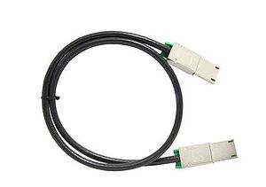
| + | Then,a PCIe x4 cable(See Figure 4-6) will be used to connect DE10-Advanced board and PCIe add-in card, the longest length is up to 3 meters.<br/> | ||
| + | ::::[[File:PCA Cable.jpg|300px]]<br/> | ||
| + | ::::::Figure 4-6 PCIe x4 cable<br/> | ||
| + | |||
| + | |||
| + | PCI Express Pin Connection is showed in Figure 4-7.<br/> | ||
| + | [[File:PCIe.jpg|500px]]<br/> | ||
| + | :::::Figure 4-7 PCI Express Pin Connection | ||
| + | <br/>These two associated devices are not included in DE10-Advanced board. To purchase the PCA card as well as the external cable, please refer to Terasic website pca.terasic.com and PCIe_Cable.terasic.com.Table 4-8 summarizes the PCI Express pin assignments of the signal names relative to the Arria 10 SoC FPGA.<br/> | ||
| + | ::::Table 4-7 PCIe Pin Assignments,Signal Names and Functions | ||
:{| class="wikitable" | :{| class="wikitable" | ||
|- | |- | ||
Revision as of 15:37, 28 August 2017
Contents |
Chapter 1 DE10-Advanced Development Kit
Terasic A10SOC is a kind of the best SoC FPGA development platform with various advanced interfaces. It built around the Intel Arria 10 SoC FPGA, which combines the dual-core ARM Cortex A9 CPU and provides 660K LEs. A10SOC has many peripherals, it can transfer data to PC with a high speed through PCIEx4 GEN3 and Type-C USB connector. The four SFP interfaces and Gigabit Ethernet port can be used in network application. HDMI 2.0 output and the two DDR4 SODIMMs allow users to deal with high bandwidth of image. A10SOC provides a FMC connector, it can extend more development space. Generally speaking, A10SoC has powerful computing and interface processing capacity, it must be the best choice for Network Communication, High Performance Computing, Image Processing and other applications.
Package Contents
The DE10-Advanced package includes:
- The DE10-Advanced board
- Quick Start Guide
- TBD
DE10-Advanced System CD
The DE10-Advanced System CD contains all the documents and supporting materials associated with DE10-Advanced, including the user manual, system builder, reference designs, and device datasheets. Users can download this system CD from the link: http://DE10-Advanced.terasic.com/cd.
Getting Help
Here are the addresses where you can get help if you encounter any problems:
Terasic Technologies
9F., No.176, Sec.2, Gongdao 5th Rd, East Dist, Hsinchu City, 30070. Taiwan
Email: support@terasic.com
Tel.: +886-3-575-0880
Website: DE10-Advanced.terasic.com
Chapter 2 Introduction of the DE10-Advanced Board
This chapter provides an introduction to the features and design characteristics of the board.
Layout and Components
Figure 2-1 and Figure 2-2 shows a photograph of the board. It depicts the layout of the board and indicates the location of the connectors and key components.

- Figure 2-1 DE10-Advanced development board (top view)

- Figure 2-2 DE10-Advanced development board (bottom view)
The DE10-Advanced board has many features that allow users to implement a wide range of designed circuits, from simple circuits to various multimedia projects. The following hardware is provided on the board:
- FPGA
- USB Type-C Interface: Power Delivery, DisplayPort TX/RX with 4 lanes, USB 3.0/2.0
- HDMI TX 2.0 for 4K2K@60. Use FPGA Transceivers
- PCIe Cabling Socket at Gen3 x4
- SFP+ Socket x4,40Gbps
- SATA 3.0 Host and SATA Device x2 (SATA connector x4)
- High Pin Count FMC Connector with transceivers. Support VADJ 1.2V/1.5V/1.8V only
- One Gigabit Ethernet Port
- On-Board 32-bit DDR4 with ECC
- DDR4 SO-DIMM Socket with ECC (up to 1066.667 MHz)
- Accelerometer, Gyroscope, Magnetometer (MPU9250)
- EPCQ1024L Serial Flash for Configuration and User Data
- Fixed and Programmable clock source for user logic, user interface, transceiver and memory
- Temperature Sensor,I2C Fan Control
- SMA Clock-In and Clock-Out.Support 1.8V I/O Standard
- LED x2, KEY x2, Switch x2, 7-Segment x2
- HPS(Hard Processor System)
- Boost Flash Slot for booting daughter card:1024 Mb QSPI Flash, NAND flash, MicroSD Socket
- DDR4 SO-DIMM Socket with ECC (up to 1066.667 MHz)
- Giga Ethernet with RJ45 connector
- USB OTG,Mini-AB USB connector
- UART-to-USB,Mini-B USB connector
- RTC
- LED x1, KEY x1
- Cold Reset and Warm Reset
Block Diagram of the DE10-Advanced Board
Figure 2-3 is the block diagram of the board. All the connections are established through the Arria 10 SoC FPGA device to provide maximum flexibility for users. Users can configure the FPGA to implement any system design.

- Figure 2-2 Block diagram of DE10-Advanced
Detailed information about Figure 2-2 are listed below.
Arria 10 SoC 10AS066K3F40E2SG/10AS057K3F40E2SG FPGA
- Dual-core ARM Cortex-A9 (HPS)
- 660K programmable logic elements
- 42,660 Kbits embedded memory
- Hard memory controllers x5
- Transceivers x48(17.4 Gbps)
- 18-bit x 19-bit multipliers x3,356
- Accelerometer & Gyroscope Device MPU9250
Configuration
- EPCQ512 Serial Configuration Device
- Onboard USB-Blaster II (Mini-B USB connector)
Memory Device
- 32GB DDR4 SDRAM on FPGA
- Two DDR3 SO-DIMM SDRAM socket
- Micro SD card socket
- 1024Mb QSPI Flash
Communication
- USB OTG (Mini-AB USB connector)
- UART-to-USB (Mini-B USB Connector)
- Giga Ethernet x2
- PCIe Gen3 x4 Cabling Socket
FMC connector
- one HPC(high-pin count) FMC connector with xcvr
- Adjustable VADJ:1.2V/1.5V/1.8V
- FMC Vita57.1 Standard
SDI connectors
- Two 12G-SDI connectors for SDI in and out
SMA connectors
- Two SMA connectors for SMA Clock-In and Clock-Out
- Support 1.8V I/O Standard
General user input/output
- Buttons x3 (FPGA x2, HPS x1)
- Switches x2 on FPGA
- LEDs x3 (FPGA x2, HPS x1)
- 7-segment displays x2
System Monitor and Control
- Temperature Sensor on FPGA
- 12V Power Monitor
- Power Controller
- I2C Fan Control
Power
- 12V DC input
Chapter 3 Board Setting and Status component
Header
Switches
LED
Chapter 4 FPGA Fabric component
USB Type C Port
USB Type-C is the new USB-IF standard that solves several challenges. It provides up to 100W power, so this board can be powered by USB type-C source and also can play a role as a USB power provider (To charge a NB or any USB type-C device up to 12V@3A). The bandwidth is double, increasing to 10Gbps with SuperSpeed+ USB3.1, and it combines multiple protocols in single cable, including DP and PCIe. And the connector is a reversible-plug connector which will be easier to use. Figure 4-1 shows the connections of USB Type C Port.Table 4-1 list the USB Type C Port assignments and signal names relative to the Arria 10 SoC FPGA.
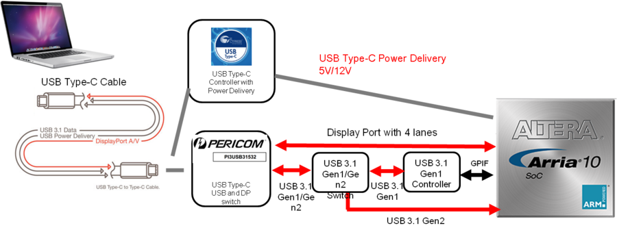
- Figure 4-1 USB Type C Port connections
- Figure 4-1 USB Type C Port connections

Table 4-1 USB Type C Port Pin Assignments, Signal Names and Functions
Signal Name FPGA Pin No. Description I/O Standard USBFX3_RESET_n PIN_AJ24 1.8V USBFX3_PCLK PIN_AT27 1.8V USBFX3_CTL0_SLCS_n PIN_AV26 1.8V USBFX3_UART_TX PIN_AP23 1.8V USBFX3_UART_RX PIN_AU27 1.8V USBFX3_CTL10 PIN_AU24 1.8V USBFX3_CTL11_A1 PIN_AU22 1.8V USBFX3_CTL12_A0 PIN_AT23 1.8V USBFX3_CTL15_INT_n PIN_AW21 1.8V USBFX3_CTL1_SLWR_n PIN_AT22 1.8V USBFX3_CTL2_SLOE_n PIN_AT25 1.8V USBFX3_CTL3_SLRD_n PIN_AR27 1.8V USBFX3_CTL4_FLAGA PIN_AN22 1.8V USBFX3_CTL5_FLAGB PIN_AN23 1.8V USBFX3_CTL6 PIN_AL24 1.8V USBFX3_CTL7_PKTEND_n PIN_AL25 1.8V USBFX3_CTL8 PIN_AV21 1.8V USBFX3_CTL9 PIN_AV22 1.8V USBFX3_DQ[0] PIN_AU21 1.8V USBFX3_DQ[1] PIN_AW23 1.8V USBFX3_DQ[2] PIN_AW24 1.8V USBFX3_DQ[3] PIN_AW25 1.8V USBFX3_DQ[4] PIN_AW26 1.8V USBFX3_DQ[5] PIN_AV24 1.8V USBFX3_DQ[6] PIN_AW28 1.8V USBFX3_DQ[7] PIN_AW30 1.8V USBFX3_DQ[8] PIN_AW29 1.8V USBFX3_DQ[9] PIN_AV27 1.8V USBFX3_DQ[10] PIN_AV28 1.8V USBFX3_DQ[11] PIN_AU26 1.8V USBFX3_DQ[12] PIN_AV23 1.8V USBFX3_DQ[13] PIN_AU25 1.8V USBFX3_DQ[14] PIN_AR25 1.8V USBFX3_DQ[15] PIN_AP24 1.8V USBFX3_DQ[16] PIN_AL23 1.8V USBFX3_DQ[17] PIN_AM24 1.8V USBFX3_DQ[18] PIN_AK25 1.8V USBFX3_DQ[19] PIN_AM25 1.8V USBFX3_DQ[20] PIN_AT24 1.8V USBFX3_DQ[21] PIN_AR26 1.8V USBFX3_DQ[22] PIN_AP26 1.8V USBFX3_DQ[23] PIN_AP25 1.8V USBFX3_DQ[24] PIN_AN24 1.8V USBFX3_DQ[25] PIN_AN26 1.8V USBFX3_DQ[26] PIN_AK23 1.8V USBFX3_DQ[27] PIN_AJ25 1.8V USBFX3_DQ[28] PIN_AJ23 1.8V USBFX3_DQ[29] PIN_AH23 1.8V USBFX3_DQ[30] PIN_AR20 1.8V USBFX3_DQ[31] PIN_AP20 1.8V
Gigabit Ethernet
The development board supports one RJ45 10/100/1000 base-T Ethernet using Marvell 88E1111. SGMII AC coupling interface is used between PHY and FPGA transceiver.The device is an auto-negotiating Ethernet PHY with an SGMII interface to the FPGA. The Arria 10 SoC FPGA can communicate with the LVDS interfaces at up to 1.6 Gbps, which is faster than 1.25 Gbps for SGMII. The MAC function must be provided in the FPGA for typical networking applications. The Marvell 88E1111 PHY uses 2.5-V and 1.1-V power rails and requires a 25MHz reference clock driven from a dedicated oscillator. It interfaces to an RJ-45 with internal magnetics for driving copper lines with Ethernet traffic.Figure 4-2 shows the SGMII interface between the FPGA and Marvell 88E1111 PHY. Table 4-2 lists the Ethernet PHY interface pin assignments.
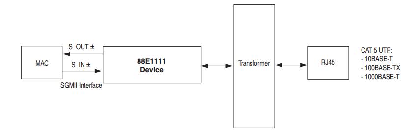
- Figure 4-2 SGMII Interface between FPGA and Marvell 88E1111 PHY

- Table 4-2 Ethernet PHY Pin Assignments, Signal Names and Functions
Signal Name FPGA Pin No. Description I/O Standard ETH_TX_p PIN_AP19 SGMII TX data LVDS ETH_RX_p PIN_AM20 SGMII RX data LVDS ETH_INT_n PIN_AU19 Management bus interrupt 1.8V ETH_MDC PIN_AT19 Management bus control 1.8V ETH_MDIO PIN_AJ20 Management bus data 1.8V ETH_RST_n PIN_AK20 Device reset 1.8V
SFP+ Connector
The development board has four independent 10G SFP+ connectors that use one transceiver channel each from the Arria 10 SoC FPGA device. These modules take in serial data from the Arria 10 SoC FPGA device and transform them to optical signals. The board includes cage assemblies for the SFP+ connectors.Figure 4-3 shows the connections between the SFP+ and Arria 10 SoC FPGA.
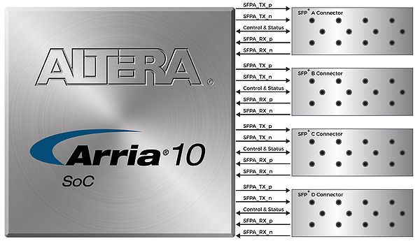
- Figure 4-3 Connection between the SFP+ and Arria 10 SoC FPGA
- Figure 4-3 Connection between the SFP+ and Arria 10 SoC FPGA

Table 4-3, Table 4-4, Table 4-5 and Table 4-6 list the four QSF+ connectors assignments and signal names relative to the Arria 10 SoC FPGA
- Table 4-3 SFP+ A Pin Assignments, Signal Names and Functions
Signal Name FPGA Pin No. Description I/O Standard SFPA_TXDISABLE PIN_W28 Turns off and disables the transmitter output 1.2 V SFPA_TXFAULT PIN_T28 Transmitter fault 1.2 V SFPA_TX_p PIN_AG37 Transmiter data HSSI DIFFERENTIAL I/O SFPA_RX_p PIN_AD35 Receiver data HSSI DIFFERENTIAL I/O SFPA_LOS PIN_G27 Signal loss indicator 1.2 V SFPA_MOD0_PRSNT_n PIN_K27 Module present 1.2 V
- Table 4-4 SFP+ B Pin Assignments, Signal Names and Functions
Signal Name FPGA Pin No. Description I/O Standard SFPB_TXDISABLE PIN_B22 Turns off and disables the transmitter output 1.2 V SFPB_TXFAULT PIN_F15 Transmitter fault 1.2 V SFPB_TX_p PIN_AF39 Transmiter data HSSI DIFFERENTIAL I/O SFPB_RX_p PIN_AC37 Receiver data HSSI DIFFERENTIAL I/O SFPB_LOS PIN_K16 Signal loss indicator 1.2 V SFPB_MOD0_PRSNT_n PIN_Y27 Module present 1.2 V
- Table 4-5 SFP+ C Pin Assignments, Signal Names and Functions
Signal Name FPGA Pin No. Description I/O Standard SFPC_TXDISABLE PIN_AN6 Turns off and disables the transmitter output 1.2 V SFPC_TXFAULT PIN_AE10 Transmitter fault 1.2 V SFPC_TX_p PIN_AE37 Transmiter data HSSI DIFFERENTIAL I/O SFPC_RX_p PIN_AC33 Receiver data HSSI DIFFERENTIAL I/O SFPC_LOS PIN_AW3 Signal loss indicator 1.2 V SFPC_MOD0_PRSNT_n PIN_AP3 Module present 1.2 V
- Table 4-6 SFP+ D Pin Assignments, Signal Names and Functions
Signal Name FPGA Pin No. Description I/O Standard SFPD_TXDISABLE PIN_M1 Turns off and disables the transmitter output 1.2 V SFPD_TXFAULT PIN_M4 Transmitter fault 1.2 V SFPD_TX_p PIN_AD39 Transmiter data HSSI DIFFERENTIAL I/O SFPD_RX_p PIN_AB35 Receiver data HSSI DIFFERENTIAL I/O SFPD_LOS PIN_T2 Signal loss indicator 1.2 V SFPD_MOD0_PRSNT_n PIN_V7 Module present 1.2 V SFP_REFCLK_p PIN_AD31 SFP reference clock LVDS SFP_MOD1_SCL PIN_AK26 Serial 2-wire clock 1.2 V SFP_MOD2_SDA PIN_AE25 Serial 2-wire data 1.2 V
SATA
The four Serial ATA (SATA) ports are available on the FPGA development board which are computer bus standard with a primary function of transferring data between the motherboard and mass storage devices (such as hard drives, optical drives, and solid-state disks). Supporting a storage interface is just one of many different applications for which an FPGA can be used in storage appliances. The Arria 10 SoC device can bridge different protocols such as bridging simple bus I/Os like PCI Express (PCIe) to SATA or network interfaces such as Gigabit Ethernet (GbE) to SATA.
The SATA interface supports SATA 3.0 standard with connection speed of 6 Gbps based on Arria 10 SoC device with integrated transceivers compliant to SATA electrical standards.
The two Serial ATA (SATA) ports include one available port for device and one available port for host capable of implementing SATA solution with a design that consists of both host and target (device side) functions.Figure 4-4 shows the connections between the SATA and Arria 10 SoC FPGA. Table 4-7 list the SATA pin assignments and signal names relative to the Arria 10 SoC FPGA.
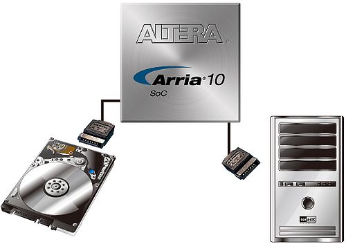
- Figure 4-4 Connection between the SATA and Arria 10 SoC FPGA
- Table 4-7 SATA Pin Assignments,Signal Names and Functions
- Figure 4-4 Connection between the SATA and Arria 10 SoC FPGA

Signal Name FPGA Pin Number Description I/O Standard SATA_HOST_REFCLK_p PIN_V31 SATA Host reference clock LVDS SATA_HOST_TX_p[0] PIN_P39 SATA Host transmitter data p[0] HSSI DIFFERENTIAL I/O SATA_HOST_TX_p[1] PIN_N37 SATA Host transmitter data p[1] HSSI DIFFERENTIAL I/O SATA_HOST_RX_p[0] PIN_U33 SATA Host Receiver data p[0] HSSI DIFFERENTIAL I/O SATA_HOST_RX_p[1] PIN_T35 SATA Host Receiver data p[1] HSSI DIFFERENTIAL I/O SATA_DEVICE_REFCLK_p PIN_M31 SATA Device reference clock LVDS SATA_DEVICE_TX_p[0] PIN_B39 SATA Device transmitter data p[0] HSSI DIFFERENTIAL I/O SATA_DEVICE_TX_p[1] PIN_A37 SATA Device transmitter data p[1] HSSI DIFFERENTIAL I/O SATA_DEVICE_RX_p[0] PIN_D35 SATA Device Receiver data p[0] HSSI DIFFERENTIAL I/O SATA_DEVICE_RX_p[1] PIN_B35 SATA Device Receiver data p[1] HSSI DIFFERENTIAL I/O
PCIe
The DE10-Advanced development board features one PCIe Express downstream interfaces (x4 lane) which are designed to interface with a PC motherboard x4 slot via PCIe cable and PCIe adapter card. Utilizing built-in transceivers on a Arria 10 SoC device, it is able to provide a fully integrated PCI Express compliant solution for multi-lane (x4) applications. With the PCI Express hard IP block incorporated in the Arria 10 SoC device, it will allow users to implement simple and fast protocols, as well as saving logic resources for logic applications.
The PCI Express interface supports complete PCI Express Gen1 at 2.5Gbps/lane, Gen2 at 5.0Gbps/lane, and Gen3 at 8.0Gbps/lane protocol stack solution compliant to PCI Express base specification 3.0 that includes PHY-MAC, Data Link, and transaction layer circuitry embedded in PCI Express hard IP blocks.
To use PCIe interface, two external associated devices will be needed to establish a link with PC. First, a PCIe half-height add-in host card with a PCIe x4 cable connector called PCA (PCIe Cabling Adapter Card and see Figure 4-5, it will be used to plug into the PCIe slot on a mother board.
- Figure 4-5 PCIe Cabling Adapter Card

Then,a PCIe x4 cable(See Figure 4-6) will be used to connect DE10-Advanced board and PCIe add-in card, the longest length is up to 3 meters.
- Figure 4-6 PCIe x4 cable
- Figure 4-6 PCIe x4 cable

PCI Express Pin Connection is showed in Figure 4-7.

- Figure 4-7 PCI Express Pin Connection
These two associated devices are not included in DE10-Advanced board. To purchase the PCA card as well as the external cable, please refer to Terasic website pca.terasic.com and PCIe_Cable.terasic.com.Table 4-8 summarizes the PCI Express pin assignments of the signal names relative to the Arria 10 SoC FPGA.
- Table 4-7 PCIe Pin Assignments,Signal Names and Functions
Signal Name FPGA Pin Number Description I/O Standard PCIE_REFCLK_p PIN_AH31 PCIe reference clock LVDS PCIE_TX_p[0] PIN_AR37 PCIe Transmitter data p0 HSSI DIFFERENTIAL I/O PCIE_TX_p[1] PIN_AP39 PCIe Transmitter data p1 HSSI DIFFERENTIAL I/O PCIE_TX_p[2] PIN_AN37 PCIe Transmitter data p2 HSSI DIFFERENTIAL I/O PCIE_TX_p[3] PIN_AM39 PCIe Transmitter data p3 HSSI DIFFERENTIAL I/O PCIE_RX_p[0] PIN_AL33 PCIe Receiver data p0 HSSI DIFFERENTIAL I/O PCIE_RX_p[1] PIN_AM35 PCIe Receiver data p1 HSSI DIFFERENTIAL I/O PCIE_RX_p[2] PIN_AJ33 PCIe Receiver data p2 HSSI DIFFERENTIAL I/O PCIE_RX_p[3] PIN_AK35 PCIe Receiver data p3 HSSI DIFFERENTIAL I/O PCIE_PERST_n PIN_AW20 PCIe present,active low 1.8 V PCIE_WAKE_n PIN_AL19 PCIe wake 1.8 V
DDR4 SO-DIMM Socket
The development board supports DDR4 SDRAM SO-DIMM. The DDR4 SODIMM socket is wired to support a maximum capacity of 8GB with a 64-bit data bus. Using differential DQS signaling for the DDR4 SDRAM interfaces, it is capable of running at up to 1067MHz memory clock. It also supports Terasic QDRII+ module and RLDRAM3 module.Figure 4-3 shows the connections between the DDR4 SDRAM SO-DIMM and Arria 10 SoC FPGA.The pin assignments for DDR4 SDRAM SO-DIMM are listed in Table 4-6.
FPGA Pin Number Signal Name Description I/O Standard PIN_AB12 DDR4A_REFCLK_p DDR4A reference clock LVDS PIN_AC1 DDR4A_A[0] Address [0] SSTL-12 PIN_AB1 DDR4A_A[1] Address [1] SSTL-12 PIN_AB4 DDR4A_A[2] Address [2] SSTL-12 PIN_AA5 DDR4A_A[3] Address [3] SSTL-12 PIN_AA3 DDR4A_A[4] Address [4] SSTL-12 PIN_AA4 DDR4A_A[5] Address [5] SSTL-12 PIN_Y2 DDR4A_A[6] Address [6] SSTL-12 PIN_AA2 DDR4A_A[7] Address [7] SSTL-12 PIN_AB5 DDR4A_A[8] Address [8] SSTL-12 PIN_AB6 DDR4A_A[9] Address [9] SSTL-12 PIN_W5 DDR4A_A[10] Address [10] SSTL-12 PIN_Y5 DDR4A_A[11] Address [11] SSTL-12 PIN_AA9 DDR4A_A[12] Address [12] SSTL-12 PIN_AB7 DDR4A_A[13] Address [13] SSTL-12 PIN_AA7 DDR4A_A[14] Address [14] SSTL-12 PIN_AB10 DDR4A_A[15] Address [15] SSTL-12 PIN_AB11 DDR4A_A[16] Address [16] SSTL-12 PIN_Y7 DDR4A_BA[0] Bank Address [0] SSTL-12 PIN_AB9 DDR4A_BA[1] Bank Address [1] SSTL-12 PIN_AA10 DDR4A_BG[0] Bank Group Inputs[0] SSTL-12 PIN_AE2 DDR4A_BG[1] Bank Group Inputs[1] SSTL-12 PIN_AD3 DDR4A_CK Clock DIFFERENTIAL 1.2-V SSTL PIN_AD4 DDR4A_CK_n Clock DIFFERENTIAL 1.2-V SSTL PIN_AC2 DDR4A_CKE Clock Enable pin 0 SSTL-12 PIN_AE8 DDR4A_DQS[0] Data Strobe p[0] DIFFERENTIAL 1.2-V POD PIN_AF7 DDR4A_DQS[1] Data Strobe p[1] DIFFERENTIAL 1.2-V POD PIN_AN1 DDR4A_DQS[2] Data Strobe p[2] DIFFERENTIAL 1.2-V POD PIN_AH2 DDR4A_DQS[3] Data Strobe p[3] DIFFERENTIAL 1.2-V POD PIN_P1 DDR4A_DQS[4] Data Strobe p[4] DIFFERENTIAL 1.2-V POD PIN_J3 DDR4A_DQS[5] Data Strobe p[5] DIFFERENTIAL 1.2-V POD PIN_R5 DDR4A_DQS[6] Data Strobe p[6] DIFFERENTIAL 1.2-V POD PIN_V9 DDR4A_DQS[7] Data Strobe p[7] DIFFERENTIAL 1.2-V POD PIN_V2 DDR4A_DQS[8] Data Strobe p[8] DIFFERENTIAL 1.2-V POD PIN_AD8 DDR4A_DQS_n[0] Data Strobe n[0] DIFFERENTIAL 1.2-V POD PIN_AE7 DDR4A_DQS_n[1] Data Strobe n[1] DIFFERENTIAL 1.2-V POD PIN_AN2 DDR4A_DQS_n[2] Data Strobe n[2] DIFFERENTIAL 1.2-V POD PIN_AH3 DDR4A_DQS_n[3] Data Strobe n[3] DIFFERENTIAL 1.2-V POD PIN_R1 DDR4A_DQS_n[4] Data Strobe n[4] DIFFERENTIAL 1.2-V POD PIN_K3 DDR4A_DQS_n[5] Data Strobe n[5] DIFFERENTIAL 1.2-V POD PIN_R6 DDR4A_DQS_n[6] Data Strobe n[6] DIFFERENTIAL 1.2-V POD PIN_W9 DDR4A_DQS_n[7] Data Strobe n[7] DIFFERENTIAL 1.2-V POD PIN_V3 DDR4A_DQS_n[8] Data Strobe n[8] DIFFERENTIAL 1.2-V POD PIN_AC11 DDR4A_DQ[0] Data [0] 1.2-V POD PIN_AD10 DDR4A_DQ[1] Data [1] 1.2-V POD PIN_AC9 DDR4A_DQ[2] Data [2] 1.2-V POD PIN_AG7 DDR4A_DQ[3] Data [3] 1.2-V POD PIN_AD13 DDR4A_DQ[4] Data [4] 1.2-V POD PIN_AD11 DDR4A_DQ[5] Data [5] 1.2-V POD PIN_AC8 DDR4A_DQ[6] Data [6] 1.2-V POD PIN_AF8 DDR4A_DQ[7] Data [7] 1.2-V POD PIN_AE6 DDR4A_DQ[8] Data [8] 1.2-V POD PIN_AJ6 DDR4A_DQ[9] Data [9] 1.2-V POD PIN_AG6 DDR4A_DQ[10] Data [10] 1.2-V POD PIN_AD6 DDR4A_DQ[11] Data [11] 1.2-V POD PIN_AG5 DDR4A_DQ[12] Data [12] 1.2-V POD PIN_AK5 DDR4A_DQ[13] Data [13] 1.2-V POD PIN_AC7 DDR4A_DQ[14] Data [14] 1.2-V POD PIN_AH6 DDR4A_DQ[15] Data [15] 1.2-V POD PIN_AK1 DDR4A_DQ[16] Data [16] 1.2-V POD PIN_AL4 DDR4A_DQ[17] Data [17] 1.2-V POD PIN_AJ4 DDR4A_DQ[18] Data [18] 1.2-V POD PIN_AM1 DDR4A_DQ[19] Data [19] 1.2-V POD PIN_AK3 DDR4A_DQ[20] Data [20] 1.2-V POD PIN_AL2 DDR4A_DQ[21] Data [21] 1.2-V POD PIN_AJ3 DDR4A_DQ[22] Data [22] 1.2-V POD PIN_AM2 DDR4A_DQ[23] Data [23] 1.2-V POD PIN_AF2 DDR4A_DQ[24] Data [24] 1.2-V POD PIN_AH1 DDR4A_DQ[25] Data [25] 1.2-V POD PIN_AG4 DDR4A_DQ[26] Data [26] 1.2-V POD PIN_AE5 DDR4A_DQ[27] Data [27] 1.2-V POD PIN_AF3 DDR4A_DQ[28] Data [28] 1.2-V POD PIN_AH4 DDR4A_DQ[29] Data [29] 1.2-V POD PIN_AG1 DDR4A_DQ[30] Data [30] 1.2-V POD PIN_AF4 DDR4A_DQ[31] Data [31] 1.2-V POD PIN_K1 DDR4A_DQ[32] Data [32] 1.2-V POD PIN_P4 DDR4A_DQ[33] Data [33] 1.2-V POD PIN_N2 DDR4A_DQ[34] Data [34] 1.2-V POD PIN_K2 DDR4A_DQ[35] Data [35] 1.2-V POD PIN_M2 DDR4A_DQ[36] Data [36] 1.2-V POD PIN_P3 DDR4A_DQ[37] Data [37] 1.2-V POD PIN_N1 DDR4A_DQ[38] Data [38] 1.2-V POD PIN_J1 DDR4A_DQ[39] Data [39] 1.2-V POD PIN_N3 DDR4A_DQ[40] Data [40] 1.2-V POD PIN_P5 DDR4A_DQ[41] Data [41] 1.2-V POD PIN_M5 DDR4A_DQ[42] Data [42] 1.2-V POD PIN_R2 DDR4A_DQ[43] Data [43] 1.2-V POD PIN_N4 DDR4A_DQ[44] Data [44] 1.2-V POD PIN_P6 DDR4A_DQ[45] Data [45] 1.2-V POD PIN_L4 DDR4A_DQ[46] Data [46] 1.2-V POD PIN_R3 DDR4A_DQ[47] Data [47] 1.2-V POD PIN_V6 DDR4A_DQ[48] Data [48] 1.2-V POD PIN_T7 DDR4A_DQ[49] Data [49] 1.2-V POD PIN_U5 DDR4A_DQ[50] Data [50] 1.2-V POD PIN_U7 DDR4A_DQ[51] Data [51] 1.2-V POD PIN_T4 DDR4A_DQ[52] Data [52] 1.2-V POD PIN_W6 DDR4A_DQ[53] Data [53] 1.2-V POD PIN_T3 DDR4A_DQ[54] Data [54] 1.2-V POD PIN_U6 DDR4A_DQ[55] Data [55] 1.2-V POD PIN_W8 DDR4A_DQ[56] Data [56] 1.2-V POD PIN_Y12 DDR4A_DQ[57] Data [57] 1.2-V POD PIN_Y11 DDR4A_DQ[58] Data [58] 1.2-V POD PIN_W10 DDR4A_DQ[59] Data [59] 1.2-V POD PIN_Y13 DDR4A_DQ[60] Data [60] 1.2-V POD PIN_Y8 DDR4A_DQ[61] Data [61] 1.2-V POD PIN_Y10 DDR4A_DQ[62] Data [62] 1.2-V POD PIN_W11 DDR4A_DQ[63] Data [63] 1.2-V POD PIN_V1 DDR4A_DQ[64] Data [64] 1.2-V POD PIN_Y1 DDR4A_DQ[65] Data [65] 1.2-V POD PIN_W3 DDR4A_DQ[66] Data [66] 1.2-V POD PIN_W1 DDR4A_DQ[67] Data [67] 1.2-V POD PIN_Y3 DDR4A_DQ[68] Data [68] 1.2-V POD PIN_W4 DDR4A_DQ[69] Data [69] 1.2-V POD PIN_U1 DDR4A_DQ[70] Data [70] 1.2-V POD PIN_U2 DDR4A_DQ[71] Data [71] 1.2-V POD PIN_AD9 DDR4A_DBI_n[0] Data Bus Inversion n[0] 1.2-V POD PIN_AJ5 DDR4A_DBI_n[1] Data Bus Inversion n[1] 1.2-V POD PIN_AK2 DDR4A_DBI_n[2] Data Bus Inversion n[2] 1.2-V POD PIN_AG2 DDR4A_DBI_n[3] Data Bus Inversion n[3] 1.2-V POD PIN_L2 DDR4A_DBI_n[4] Data Bus Inversion n[4] 1.2-V POD PIN_L3 DDR4A_DBI_n[5] Data Bus Inversion n[5] 1.2-V POD PIN_U4 DDR4A_DBI_n[6] Data Bus Inversion n[6] 1.2-V POD PIN_V8 DDR4A_DBI_n[7] Data Bus Inversion n[7] 1.2-V POD PIN_V4 DDR4A_DBI_n[8] Data Bus Inversion n[8] 1.2-V POD PIN_AE1 DDR4A_CS_n Chip Select SSTL-12 PIN_AE3 DDR4A_RESET_n Chip Reset 1.2 V PIN_AC3 DDR4A_ODT On Die Termination SSTL-12 PIN_AC6 DDR4A_PAR Command and Address Parity Input SSTL-12 PIN_AC12 DDR4A_ALERT_n Alert SSTL-12 PIN_AD1 DDR4A_ACT_n Activation Command Input SSTL-12 PIN_T5 DDR4A_EVENT_n Chip Temperature Event 1.2 V PIN_AD5 DDR4A_AC_R[0] SSTL-12 PIN_Y6 DDR4A_AC_R[1] SSTL-12 PIN_AC4 DDR4A_C[0] SSTL-12 PIN_AB2 DDR4A_C[1] SSTL-12 PIN_AA8 DDR4A_RZQ 1.2 V
HDMI
The development board provides High Performance HDMI Transmitter via the devices SN75DP159 which incorporates HDMI v1.4b and v2.0a features, including Ultra HD video and HDTV support. The SN75DP159 is controlled via a serial I2C bus interface, which is connected to pins on the Arria 10 SoC FPGA.The pin assignment associated to HDMI port is listed in table below.
Signal Name FPGA Pin Number Description I/O Standard HDMI_REFCLK_p PIN_Y31 Video reference Clock LVDS HDMI_TX_CLK_p PIN_V39 Video Clock HSSI DIFFERENTIAL I/O HDMI_TX_D_p[0] PIN_U37 Video Data bus p[0] HSSI DIFFERENTIAL I/O HDMI_TX_D_p[1] PIN_T39 Video Data bus p[1] HSSI DIFFERENTIAL I/O HDMI_TX_D_p[2] PIN_R37 Video Data bus p[2] HSSI DIFFERENTIAL I/O
Display Port
The DE10-Advanced board includes a DisplayPort connector. We plan to support DisplayPort both source and sink port on USB Type-C connector:support DisplayPort 1.2a spec and data rate up to 5.4Gbps per lane, 4 lanes in total.
Signal Name FPGA Pin No. Description I/O Standard DP_REFCLK_p PIN_AM31 Display reference clock LVDS DP_TX_p[0] PIN_AW37 Transmitter data p0 HSSI DIFFERENTIAL I/O DP_TX_p[1] PIN_AV39 Transmitter data p1 HSSI DIFFERENTIAL I/O DP_TX_p[2] PIN_AU37 Transmitter data p2 HSSI DIFFERENTIAL I/O DP_TX_p[3] PIN_AT39 Transmitter data p3 HSSI DIFFERENTIAL I/O DP_RX_p[0] PIN_AV35 Receiver data p0 HSSI DIFFERENTIAL I/O DP_RX_p[1] PIN_AT35 Receiver data p1 HSSI DIFFERENTIAL I/O DP_RX_p[2] PIN_AN33 Receiver data p2 HSSI DIFFERENTIAL I/O DP_RX_p[3] PIN_AP35 Receiver data p3 HSSI DIFFERENTIAL I/O DP_AUX_p PIN_AM22 Display port AUX port 1.8V