DE10-Advanced revC demo: PCIe Reference Design - Fundamental
From Terasic Wiki
(Difference between revisions)
(→FPGA Application Design) |
(→FPGA Application Design) |
||
| Line 62: | Line 62: | ||
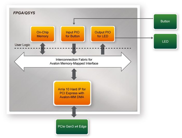
[[#Figure715|Figure 1-6]] shows the system block diagram in the FPGA system. In the Qsys, Altera PIO controller is used to control the LED and monitor the Button Status, and the On-Chip memory is used for performing DMA testing. The PIO controllers and the On-Chip memory are connected to the PCI Express Hard IP controller through the Memory-Mapped Interface. | [[#Figure715|Figure 1-6]] shows the system block diagram in the FPGA system. In the Qsys, Altera PIO controller is used to control the LED and monitor the Button Status, and the On-Chip memory is used for performing DMA testing. The PIO controllers and the On-Chip memory are connected to the PCI Express Hard IP controller through the Memory-Mapped Interface. | ||
| - | + | [[Image: DE10-Advanced_revC_PCIE_pic_15.png|600px]] | |
| - | + | ::::'''Figure 1-6 Hardware block diagram of the PCIe reference design''' | |
=Windows Based Application Software Design= | =Windows Based Application Software Design= | ||
Revision as of 16:28, 27 August 2018
The application reference design shows how to implement fundamental control and data transfer in DMA. In the design, basic I/O is used to control the BUTTON and LED on the FPGA board. High-speed data transfer is performed by DMA.
Contents |
Demonstration Files Location
The demo file is located in the batch folder: CDROM\Demonstrations\ PCIe_Fundamental\demo_batch
The folder includes following files:
- FPGA Configuration File: PCIe_Fundamental.sof
- Download Batch file: test.bat
- Windows Application Software folder : windows_app, includes
- PCIE_FUNDAMENTAL.exe
- TERASIC_PCIE_AVMM.DLL
Demonstration Setup
- Install the FPGA board on your PC as shown in Figure 1-1.
- Configure FPGA with PCIe_Fundamental.sof by executing the test.bat.
- Install PCIe driver if necessary. The driver is located in the folder: CDROM\Demonstration\PCIe_SW_KIT\Windows\PCIe_Driver.
- Make sure the Windows has detected the FPGA Board by checking the Windows Control panel as shown in Figure 1-1.
-
- Figure 1-1 Screenshot for PCIe Driver
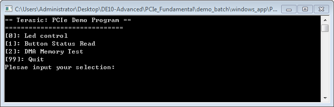
- Goto windows_app folder, execute PCIE_FUNDAMENTAL.exe. A menu will appear as shown in Figure 1-2.
-
- Figure 1-2 Screenshot of Program Menu
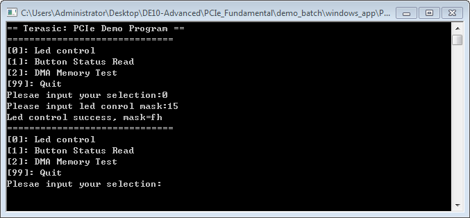
- Type 0 followed by a ENTER key to select Led Control item, then input 15 (hex 0x0f) will make all led on as shown in Figure 1-3. If input 0 (hex 0x00), all led will be turn off.
-
- Figure 1-3 Screenshot of LED Control
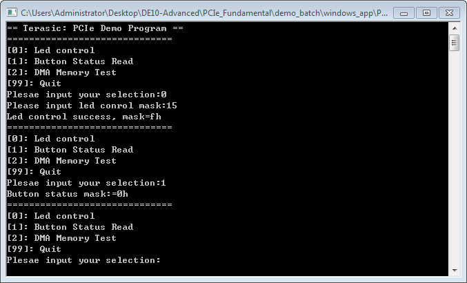
- Type 1 followed by an ENTER key to select Button Status Read item. The button status will be report as shown in Figure 1-4.
-
- Figure 1-4 Screenshot of Button Status Report
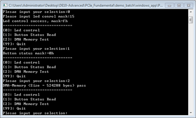
- Type 2 followed by an ENTER key to select DMA Testing item. The DMA test result will be report as shown in Figure 1-5.
-
- Figure 1-5 Screenshot of DMA Memory Test Result
- Type 99 followed by an ENTER key to exit this test program


Development Tools
- Quartus Prime 18.0 Standard Edition
- Visual C++ 2012
Demonstration Source Code Location
- Quartus Project: Demonstrations\PCIe_Fundamental
- C++ Project: Demonstrations\PCIe_SW_KIT\Windows\PCIE_FUNDAMENTAL
FPGA Application Design
Figure 1-6 shows the system block diagram in the FPGA system. In the Qsys, Altera PIO controller is used to control the LED and monitor the Button Status, and the On-Chip memory is used for performing DMA testing. The PIO controllers and the On-Chip memory are connected to the PCI Express Hard IP controller through the Memory-Mapped Interface.

- Figure 1-6 Hardware block diagram of the PCIe reference design
Windows Based Application Software Design
The application software project is built by Visual C++ 2012. The project includes the following major files:
| Name | Description |
| PCIE_FUNDAMENTAL.cpp | Main program |
| PCIE.c | Implement dynamically load for TERAISC_PCIE_AVMM.DLL |
| PCIE.h | |
| TERASIC_PCIE_AVMM.h | SDK library file, defines constant and data structure |
The main program PCIE_FUNDAMENTAL.cpp includes the header file "PCIE.h" and defines the controller address according to the FPGA design.
The base address of BUTTON and LED controllers are 0x4000010 and 0x4000020 based on PCIE_BAR4, in respectively. The on-chip memory base address is 0x00000000 relative to the DMA controller.
Before accessing the FPGA through PCI Express, the application first calls PCIE_Load to dynamically load the TERASIC_PCIE_AVMM.dll. Then, it call PCIE_Open to open the PCI Express driver. The constant DEFAULT_PCIE_VID and DEFAULT_PCIE_DID used in PCIE_Open are defined in TERASIC_PCIE_AVMM.h. If developer change the Vendor ID and Device ID and PCI Express IP, they also need to change the ID value define in TERASIC_PCIE_AVMM.h. If the return value of PCIE_Open is zero, it means the driver cannot be accessed successfully. In this case, please make sure:
* The FPGA is configured with the associated bit-stream file and the host is rebooted.
- The PCI express driver is loaded successfully.
The LED control is implemented by calling PCIE_Write32 API, as shown below:
| 500px |
The button status query is implemented by calling the PCIE_Read32 API, as shown below:
| 500px |
The memory-mapped memory read and write test is implemented by PCIE_DmaWrite and PCIE_DmaRead API, as shown below: