DE10-Advance Hardware Manual revC Chapter4 USB Type C Port
From Terasic Wiki
Contents |
4.1 USB Type C Port
The DE10-Advanced board features one USB Type C connector. It is designed for high-speed data transmission with computers and image output applications. Figure 4-1 shows the block diagram of the connection between USB Type C port and FPGA.
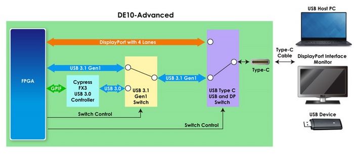
- Figure 4-1 Block diagram of the connection between USB Type C port and FPGA

As shown in Figure 4-1, it connects to FPGA through several switch circuits and USB controllers, users can switch USB Type C connector to a variety of applications as below:
- USB 3.0 Device to USB Host PC
- USB 2.0 OTG
- DisplayPort Source Application (Need DP Source IP)
- USB 3.1 Gen1 Application (Need USB 3.1 Gen1 IP)
We will describe the circuits diagram and these functions in detail below.
4.1.1 Display Port
As shown in Figure 3-2,USB type C port can connect to FPGA transceiver. Users can implement a Display port source mode IP in FPGA, the DE10-Advanced board will implement the features of display port source.
Through the USB Type C cable, users can connect DE10-Advanced board to the monitor which supports Display port interface. Then the image processed by FPGA can be displayed on the monitor.
Th display port provides data rate up to 5.4Gbps per lane and 4 lanes in total, it supports DisplayPort 1.2a Spec.
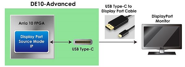
- Figure 4-2 USB Type-C Application : DisplayPort TX Source

- Table 4-1 DisplayPort Signal Names and Functions
Signal Name FPGA Pin Number Description I/O Standard DP_REFCLK_p AM31 Display reference clock form PLL LVDS DP_TX_p[0] AW37 TX Lane 1 HSSI Differential I/O DP_TX_p[1] AV39 TX Lane 2 HSSI Differential I/O DP_TX_p[2] AU37 TX Lane 3 HSSI Differential I/O DP_TX_p[3] AT39 TX Lane 4 HSSI Differential I/O DP_AUX_p AM22 Display port AUX port DIFFERENTIAL 1.8-V SSTL CLASS I DP_DX_SEL AB27 Display Port channel TX or RX(Reserve) select.
DP_DX_SEL = 0 : USB TypeC in Display TX mode .
DP_DX_SEL = 1(Reserve) : USB TypeC in Display RX mode1.8 V DP_AUX_SEL AC28 AUX/DDC Selection Control Pin in Conjunction with Dx_SEL Pin 1.8 V USBDP_SW_CNF0 AA27 TX Lane 1 1.8V USBDP_SW_CNF1 AB26 TX Lane 1 1.8V USBDP_SW_CNF2 AB25 TX Lane 1 1.8V
4.1.2 USB 3.0 Device
The DE10-Advanced board has one Cypress FX3 USB Controller(CYUSB3014).The USB controller is connected to FPGA through the programmable GPIF II interface, and connect to the external USB Type C connector, It provides USB 3.0 Device application for DE10-Advanced board.
As shown in Figure 4-3, users can connect FX3 USB Controller to PC through USB Type C cable, and transfer USB 3.0 data between FPGA and USB Host PC with transfer rate 320MByte/s (Using the demonstration provided by Cypress).
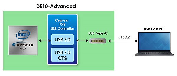
- Figure 4-3 FX3 USB 3.0 Controller application

4.1.3 USB 2.0 OTG
The Cypress FX3 USB controller also has a USB 2.0 OTG controller. It allows the DE10-Advanced board function as an OTG Host to MSC as well as HID-class devices, as shown in Figure 4-4.
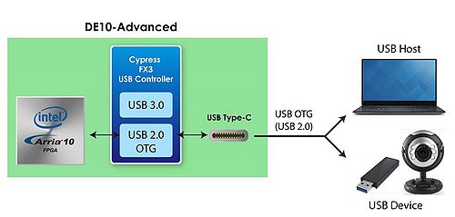
- Figure 4-4 USB 2.0 OTG Controller application

- Table 4-2 FX3 USB 3.0 Controller Signal Names and Functions
| Signal Name | FPGA Pin Number | Description | I/O Standard |
|---|---|---|---|
| USBFX3_DQ[0] | AU21 | GPIF II Data Bus 0 | 1.8 V |
| USBFX3_DQ[1] | AW23 | GPIF II Data Bus 1 | 1.8 V |
| USBFX3_DQ[2] | AW24 | GPIF II Data Bus 2 | 1.8 V |
| USBFX3_DQ[3] | AW25 | GPIF II Data Bus 3 | 1.8 V |
| USBFX3_DQ[4] | AW26 | GPIF II Data Bus 4 | 1.8 V |
| USBFX3_DQ[5] | AV24 | GPIF II Data Bus 5 | 1.8 V |
| USBFX3_DQ[6] | AW28 | GPIF II Data Bus 6 | 1.8 V |
| USBFX3_DQ[7] | AW30 | GPIF II Data Bus 7 | 1.8 V |
| USBFX3_DQ[8] | AW29 | GPIF II Data Bus 8 | 1.8 V |
| USBFX3_DQ[9] | AV27 | GPIF II Data Bus 9 | 1.8 V |
| USBFX3_DQ[10] | AV28 | GPIF II Data Bus 10 | 1.8 V |
| USBFX3_DQ[11] | AU26 | GPIF II Data Bus 11 | 1.8 V |
| USBFX3_DQ[12] | AV23 | GPIF II Data Bus 12 | 1.8 V |
| USBFX3_DQ[13] | AU25 | GPIF II Data Bus 13 | 1.8 V |
| USBFX3_DQ[14] | AR25 | GPIF II Data Bus 14 | 1.8 V |
| USBFX3_DQ[15] | AP24 | GPIF II Data Bus 15 | 1.8 V |
| USBFX3_DQ[16] | AL23 | GPIF II Data Bus 16 | 1.8 V |
| USBFX3_DQ[17] | AM24 | GPIF II Data Bus 17 | 1.8 V |
| USBFX3_DQ[18] | AK25 | GPIF II Data Bus 18 | 1.8 V |
| USBFX3_DQ[19] | AM25 | GPIF II Data Bus 19 | 1.8 V |
| USBFX3_DQ[20] | AT24 | GPIF II Data Bus 20 | 1.8 V |
| USBFX3_DQ[21] | AR26 | GPIF II Data Bus 21 | 1.8 V |
| USBFX3_DQ[22] | AP26 | GPIF II Data Bus 22 | 1.8 V |
| USBFX3_DQ[23] | AP25 | GPIF II Data Bus 23 | 1.8 V |
| USBFX3_DQ[24] | AN24 | GPIF II Data Bus 24 | 1.8 V |
| USBFX3_DQ[25] | AN26 | GPIF II Data Bus 25 | 1.8 V |
| USBFX3_DQ[26] | AK23 | GPIF II Data Bus 26 | 1.8 V |
| USBFX3_DQ[27] | AJ25 | GPIF II Data Bus 27 | 1.8 V |
| USBFX3_DQ[28] | AJ23 | GPIF II Data Bus 28 | 1.8 V |
| USBFX3_DQ[29] | AH23 | GPIF II Data Bus 29 | 1.8 V |
| USBFX3_DQ[30] | AR20 | GPIF II Data Bus 30 | 1.8 V |
| USBFX3_DQ[31] | AP20 | GPIF II Data Bus 31 | 1.8 V |
| USBFX3_CTL0_SLCS_n | AV26 | GPIF II Control Bus 0 | 1.8 V |
| USBFX3_CTL1_SLWR_n | AT22 | GPIF II Control Bus 1 | 1.8 V |
| USBFX3_CTL2_SLOE_n | AT25 | GPIF II Control Bus 2 | 1.8 V |
| USBFX3_CTL3_SLRD_n | AR27 | GPIF II Control Bus 3 | 1.8 V |
| USBFX3_CTL4_FLAGA | AN22 | GPIF II Control Bus 4 | 1.8 V |
| USBFX3_CTL5_FLAGB | AN23 | GPIF II Control Bus 5 | 1.8 V |
| USBFX3_CTL6 | AL24 | GPIF II Control Bus 6 | 1.8 V |
| USBFX3_CTL7_PKTEND_n | AL25 | GPIF II Control Bus 7 | 1.8 V |
| USBFX3_CTL8 | AV21 | GPIF II Control Bus 8 | 1.8 V |
| USBFX3_CTL9 | AV22 | GPIF II Control Bus 9 | 1.8 V |
| USBFX3_CTL10 | AU24 | GPIF II Control Bus 10 | 1.8 V |
| USBFX3_CTL11_A1 | AU22 | GPIF II Control Bus 11 | 1.8 V |
| USBFX3_CTL12_A0 | AT23 | GPIF II Control Bus 12 | 1.8 V |
| USBFX3_CTL15_INT_n | AW21 | GPIF II Control Bus 15 | 1.8 V |
| USBFX3_RESET_n | AJ24 | FX3 reset | 1.8 V |
| USBFX3_PCLK | AT27 | FX3 clok | 1.8 V |
| USBFX3_UART_TX | AP23 | USB to UART transmitter | 1.8 V |
| USBFX3_UART_RX | AU27 | USB to UART receiver | 1.8 V |
| USBFX3_OTG_ID | AG26 | OTG ID pin | 1.8 V |
4.1.4 USB 3.1 Gen1 Application
As shown in Figure 4-5, user can implement an independent or a third-party USB 3.1 Host or Device IP in FPGA. Through the circuit of FPGA and USB type C connector, the FPGA transceiver can connect to USB Type C connector and achieve the USB 3.o or USB 3.1 Host or Device application.
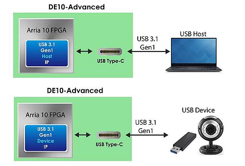
- Figure 4-5 Using USB 3.1 Gen 1 IP

- Table 4-3 USB 3.1 Gen 1 application Signal Names and Functions
Signal Name FPGA Pin Number Description I/O Standard USB_REFCLK_p AB31 USB usb reference clock LVDS USB_TX_p AB39 USB 3.1 Interface transmitter line HSSI Differential I/O USB_RX_p AA37 USB 3.1 Interface receiver line HSSI Differential I/O
4.1.5 Power Application
The DE10-Advanced board also can be powered through USB Type C port with USB Type C power adpater. The adapter with power above 80W is recommended for DE10-Advanced board.
Note: Make sure the USB to UART connector (J27) is not connected before using the power adapter, or the DE10-Advanced board can't be power on normally. User can use J27 after the board is powered on.