DE10-Advance Hardware Manual revC Chapter4 SATA
From Terasic Wiki
4.4 SATA
Four Serial ATA (SATA) ports are available on the FPGA development board which are computer bus standard with a primary function of transferring data between the motherboard and mass storage devices (such as hard drives, optical drives, and solid-state disks). Supporting a storage interface is just one of many different applications an FPGA can be used in storage appliances. The Arria 10 SoC device can bridge different protocols such as bridging simple bus I/Os like PCI Express (PCIe) to SATA or network interfaces such as Gigabit Ethernet (GbE) to SATA. The SATA interface supports SATA 3.0 standard with connection speed of 6 Gbps based on Arria 10 SoC device with integrated transceivers compliant to SATA electrical standards.
The four Serial ATA (SATA) ports include two available ports for device and two available ports for host capable of implementing SATA solution with a design that consists of both host and target(device side) functions.Figure 4-4 depicts the host and device design examples.
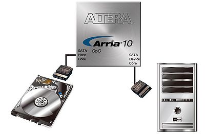
- Figure 4-4 PC and storage device connection to the Arria 10 SoC FPGA
- Figure 4-4 PC and storage device connection to the Arria 10 SoC FPGA

The transmitter and receiver signals of the SATA ports are connected directly to the Arria 10 SoC transceiver channels to provide SATA IO connectivity to both host and target devices. To verify the functionality of the SATA host/device ports, a connection can be established between the two ports by using a SATA cable as Figure 4-5 depicts the associated signals connected.Table 4-7 lists the SATA pin assignments, signal names and functions.
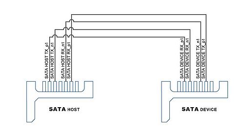
- Figure 4-5 Pin connection between SATA connectors
- Figure 4-5 Pin connection between SATA connectors
- Table 4-7 SATA Pin Assignments,Signal Names and Functions

Signal Name FPGA Pin Number Description I/O Standard Device SATA_DEVICE_REFCLK_p PIN_M31 SATA Device reference clock LVDS SATA_DEVICE_REFCLK_n PIN_M30 SATA Device reference clock LVDS SATA_DEVICE_RX_n0 PIN_D34 Differential receive data input after DC blocking capacitor HSSI DIFFERENTIAL I/O SATA_DEVICE_RX_n1 PIN_B34 Differential receive data input after DC blocking capacitor HSSI DIFFERENTIAL I/O SATA_DEVICE_TX_n0 PIN_B38 Differential transmit data output before DC blocking capacitor HSSI DIFFERENTIAL I/O SATA_DEVICE_TX_n1 PIN_A36 Differential transmit data output before DC blocking capacitor HSSI DIFFERENTIAL I/O SATA_DEVICE_TX_p0 PIN_B39 Differential transmit data output before DC blocking capacitor HSSI DIFFERENTIAL I/O SATA_DEVICE_TX_p1 PIN_A37 Differential transmit data output before DC blocking capacitor HSSI DIFFERENTIAL I/O SATA_DEVICE_RX_p0 PIN_D35 Differential receive data input after DC blocking capacitor HSSI DIFFERENTIAL I/O SATA_DEVICE_RX_p1 PIN_B35 Differential receive data input after DC blocking capacitor HSSI DIFFERENTIAL I/O Host SATA_HOST_REFCLK_p PIN_AF31 SATA Host reference clock LVDS SATA_HOST_REFCLK_n PIN_AF30 SATA Host reference clock LVDS SATA_HOST_TX_p0 PIN_AJ37 Differential transmit data output before DC blocking capacitor HSSI DIFFERENTIAL I/O SATA_HOST_TX_p1 PIN_AH39 Differential transmit data output before DC blocking capacitor HSSI DIFFERENTIAL I/O SATA_HOST_RX_p0 PIN_AE33 Differential receive data input after DC blocking capacitor HSSI DIFFERENTIAL I/O SATA_HOST_RX_p1 PIN_AF35 Differential receive data input after DC blocking capacitor HSSI DIFFERENTIAL I/O SATA_HOST_TX_n0 PIN_AJ36 Differential transmit data output before DC blocking capacitor HSSI DIFFERENTIAL I/O SATA_HOST_TX_n1 PIN_AH38 Differential transmit data output before DC blocking capacitor HSSI DIFFERENTIAL I/O SATA_HOST_RX_n0 PIN_AE32 Differential receive data input after DC blocking capacitor HSSI DIFFERENTIAL I/O SATA_HOST_RX_n1 PIN_AF34 Differential receive data input after DC blocking capacitor HSSI DIFFERENTIAL I/O