DE-Core Reserve Area manual
From Terasic Wiki
(Difference between revisions)
| (13 intermediate revisions not shown) | |||
| Line 1: | Line 1: | ||
=='''The Reserved GPIO'''== | =='''The Reserved GPIO'''== | ||
| - | The board has 1x7 3x4 and 2x4 reserved GPIO pads. These GPIOs are connected to MAX 10 FPGA device directly. Figure | + | The board has 1x7 3x4 and 2x4 reserved GPIO pads. These GPIOs are connected to MAX 10 FPGA device directly. '''Figure 1''' shows the connection between the GPIO pads and MAX 10 FPGA. '''Figure 2''' shows the Pin-outs of the reserved GPIO Pads. '''Table 1''' shows the pin assignment of the reserved GPIOs. |
| - | [[File:DE-Core_manual_reserved_GPIO2.jpg| | + | [[File:DE-Core_manual_reserved_GPIO2.jpg|650px]] |
| - | '''Connection Between the GPIO Pads and MAX 10 FPGA''' | + | '''Figure 1 Connection Between the GPIO Pads and MAX 10 FPGA''' |
| - | [[File:DE-Core_manual_reserved_GPIO1.jpg| | + | [[File:DE-Core_manual_reserved_GPIO1.jpg|650px]] |
| - | '''Pin-outs of the reserved GPIO Pads''' | + | '''Figure 2 Pin-outs of the reserved GPIO Pads''' |
| - | '''Table | + | '''Table 1 Pin Assignment of the reserved GPIO''' |
{| class="wikitable" | {| class="wikitable" | ||
Latest revision as of 10:11, 10 July 2019
The Reserved GPIO
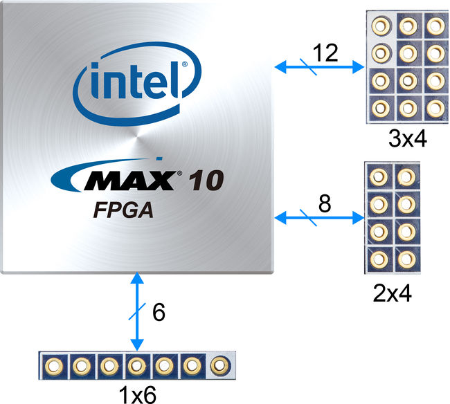
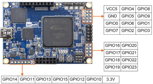
The board has 1x7 3x4 and 2x4 reserved GPIO pads. These GPIOs are connected to MAX 10 FPGA device directly. Figure 1 shows the connection between the GPIO pads and MAX 10 FPGA. Figure 2 shows the Pin-outs of the reserved GPIO Pads. Table 1 shows the pin assignment of the reserved GPIOs.
Figure 1 Connection Between the GPIO Pads and MAX 10 FPGA
Figure 2 Pin-outs of the reserved GPIO Pads
Table 1 Pin Assignment of the reserved GPIO
| Signal Name | FPGA Pin No. | Description | I/O Standard |
|---|---|---|---|
| GPIO0 | PIN_H21 | GPIO Connection [0] | 3.3-V LVTTL |
| GPIO1 | PIN_H22 | GPIO Connection [1] | 3.3-V LVTTL |
| GPIO2 | PIN_J21 | GPIO Connection [2] | 3.3-V LVTTL |
| GPIO3 | PIN_J22 | GPIO Connection [3] | 3.3-V LVTTL |
| GPIO4 | PIN_G19 | GPIO Connection [4] | 3.3-V LVTTL |
| GPIO5 | PIN_G20 | GPIO Connection [5] | 3.3-V LVTTL |
| GPIO6 | PIN_F22 | GPIO Connection [6] | 3.3-V LVTTL |
| GPIO7 | PIN_G22 | GPIO Connection [7] | 3.3-V LVTTL |
| GPIO8 | PIN_E21 | GPIO Connection [8] | 3.3-V LVTTL |
| GPIO9 | PIN_E22 | GPIO Connection [9] | 3.3-V LVTTL |
| GPIO10 | PIN_Y4 | GPIO Connection [10] | 3.3-V LVTTL |
| GPIO11 | PIN_AA1 | GPIO Connection [11] | 3.3-V LVTTL |
| GPIO12 | PIN_Y3 | GPIO Connection [12] | 3.3-V LVTTL |
| GPIO13 | PIN_Y2 | GPIO Connection [13] | 3.3-V LVTTL |
| GPIO14 | PIN_Y1 | GPIO Connection [14] | 3.3-V LVTTL |
| GPIO15 | PIN_AA2 | GPIO Connection [15] | 3.3-V LVTTL |
| GPIO16 | PIN_T22 | GPIO Connection [16] | 3.3-V LVTTL |
| GPIO17 | PIN_AA21 | GPIO Connection [17] | 3.3-V LVTTL |
| GPIO18 | PIN_T21 | GPIO Connection [18] | 3.3-V LVTTL |
| GPIO19 | PIN_T19 | GPIO Connection [19] | 3.3-V LVTTL |
| GPIO20 | PIN_U22 | GPIO Connection [20] | 3.3-V LVTTL |
| GPIO21 | PIN_AA22 | GPIO Connection [21] | 3.3-V LVTTL |
| GPIO22 | PIN_U21 | GPIO Connection [22] | 3.3-V LVTTL |
| GPIO23 | PIN_T20 | GPIO Connection [23] | 3.3-V LVTTL |

