DE10-Advance Hardware Manual revC Chapter3 JTAG Interface
From Terasic Wiki
(Difference between revisions)
(Created page with "==3.4 JTAG Interface== Figure 3-2 shows the JTAG interface of DE10-Advanced.Users can access to the JTAG interface through the USB Blaster II circuit or connect external blaster ...") |
(→3.4 JTAG Interface) |
||
| Line 5: | Line 5: | ||
[[File:De10 advanced revc jtagchain.jpg|500px]] | [[File:De10 advanced revc jtagchain.jpg|500px]] | ||
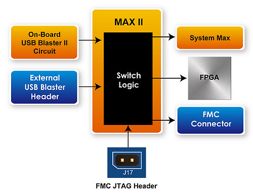
::::::'''Figure 3-2 JTAG interface of DE10-Advanced''' | ::::::'''Figure 3-2 JTAG interface of DE10-Advanced''' | ||
| + | |||
| + | [[DE10-Advance Hardware Manual revC Chapter3|'''Back''']] | ||
Latest revision as of 17:51, 29 August 2018
3.4 JTAG Interface
Figure 3-2 shows the JTAG interface of DE10-Advanced.Users can access to the JTAG interface through the USB Blaster II circuit or connect external blaster to external blaster header.All the devices which implement JTAG are connect to MAX II device,and switch via MAX II internal switch logic.By using headers J17,users can include FMC connector JTAG interface in the DE10-Advanced JTAG Chain,or exclude them from the JTAG Chain.The default JTAG path for de10-advanced is: USB Blaster II ==> HPS ==> FPGA ==> (Bypass FMC connector) ==> USB Blaster II.When the External JTAG connector is connected to the external blaster, the On board's USB blaster II function will be replaced by the external blaster.
- Figure 3-2 JTAG interface of DE10-Advanced
