DE10-Advanced User Manual
From Terasic Wiki
(→1.2 DE10-Advanced System CD) |
(→1.3 Getting Help) |
||
| Line 11: | Line 11: | ||
The DE10-Advanced System CD contains all the documents and supporting materials associated with DE10-Advanced, including the user manual, system builder, reference designs, and device datasheets. Users can download this system CD from the link: http://DE10-Advanced.terasic.com/cd. | The DE10-Advanced System CD contains all the documents and supporting materials associated with DE10-Advanced, including the user manual, system builder, reference designs, and device datasheets. Users can download this system CD from the link: http://DE10-Advanced.terasic.com/cd. | ||
| - | == | + | ==Getting Help== |
Here are the addresses where you can get help if you encounter any problems: | Here are the addresses where you can get help if you encounter any problems: | ||
Revision as of 16:01, 3 August 2017
Contents |
Chapter 1 DE10-Advanced Development Kit
Terasic A10SOC is a kind of the best SoC FPGA development platform with various advanced interfaces. It built around the Intel Arria 10 SoC FPGA, which combines the dual-core ARM Cortex A9 CPU and provides 660K LEs. A10SOC has many peripherals, it can transfer data to PC with a high speed through PCIEx4 GEN3 and Type-C USB connector. The four SFP interfaces and Gigabit Ethernet port can be used in network application. HDMI 2.0 output and the two DDR4 SODIMMs allow users to deal with high bandwidth of image. A10SOC provides a FMC connector, it can extend more development space. Generally speaking, A10SoC has powerful computing and interface processing capacity, it must be the best choice for Network Communication, High Performance Computing, Image Processing and other applications.
Package Contents
The DE10-Advanced package includes:
- The DE10-Advanced board
- Quick Start Guide
- TBD
DE10-Advanced System CD
The DE10-Advanced System CD contains all the documents and supporting materials associated with DE10-Advanced, including the user manual, system builder, reference designs, and device datasheets. Users can download this system CD from the link: http://DE10-Advanced.terasic.com/cd.
Getting Help
Here are the addresses where you can get help if you encounter any problems:
Terasic Technologies
9F., No.176, Sec.2, Gongdao 5th Rd, East Dist, Hsinchu City, 30070. Taiwan
Email: support@terasic.com
Tel.: +886-3-575-0880
Website: DE10-Advanced.terasic.com
Chapter 2 Introduction of the DE10-Advanced Board
This chapter provides an introduction to the features and design characteristics of the board.
2.1 Layout and Components
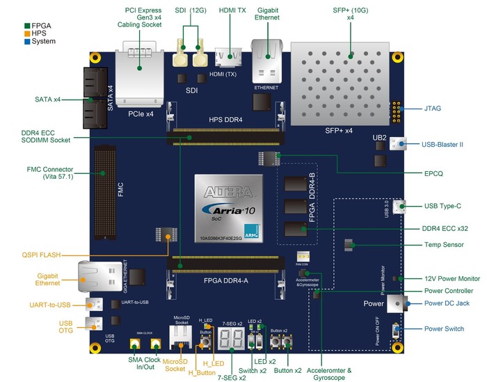
Figure 2-1 shows a photograph of the board. It depicts the layout of the board and indicates the location of the connectors and key components.
- Figure 2-1 DE10-Advanced development board (top view)
The DE10-Advanced board has many features that allow users to implement a wide range of designed circuits, from simple circuits to various multimedia projects. The following hardware is provided on the board:
- FPGA
- USB Type-C Interface - Power Delivery, DisplayPort TX/RX with 4 lanes & USB 3.0/2.0
- HDMI 2.0 for 4K2K@60- FPGA Transceiver
- PCIe Cabling Socket at Gen3 x4
- SFP+ Socket x4,40Gbps
- SATA 3.0 Host and SATA Device x2 (SATA connectors x4)
- FMC connector x1 with xcvr(High Pin Count).Support VADJ 1.2V/1.5V/1.8V only
- One Gigabit Ethernet Port
- DDR4 SO-DIMM Socket x2 with ECC (up to 1066.667MHz)
- Accelerometer and Gyroscope (MPU9250)
- EPCQ512 Serial Flash for Configuration and User Data
- Fixed and Programmable clock source for user logic,user interface,xcvr and memory
- Temperature Sensor,I2C Fan Control
- SMA Clock-In and Clock-Out.Support 1.8V I/O Standard
- LEDs x2,Buttons x2,Switches x2,7-Seg x2
- On Board USB Blaster II
- HPS(Hard Processor System)
- 1024 Mb QSPI Flash,nand flash,MicroSD Socket for boot and data (Boost Flash Slot,same as Altera Arria10 SoC board)
- DDR4 x72 with ECC,4GB at 1067 MHz (up to 4GB)
- Giga Ethernet with RJ45 connector
- USB OTG,Mini-AB USB connector
- UART-to-USB,Mini-B USB connector
- RTC
- LED x1,Button x1
- Cold Reset and Warm Reset
2.2 Block Diagram of the DE10-Advanced Board
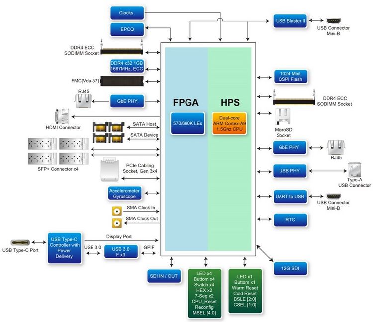
Figure 2-2 is the block diagram of the board. All the connections are established through the Arria 10 SoC FPGA device to provide maximum flexibility for users. Users can configure the FPGA to implement any system design.
- Figure 2-2 Block diagram of DE10-Advanced
Detailed information about Figure 2-2 are listed below.
Arria 10 SoC 10AS066K3F40E2SG FPGA
- Dual-core ARM Cortex-A9 (HPS)
- 660K programmable logic elements
- 42,660 Kbits embedded memory
- Hard memory controllers x5
- Transceivers x48(17.4 Gbps)
- 18-bit x 19-bit multipliers x3,356
- Accelerometer & Gyroscope Device MPU9250
Configuration
- EPCQ512 Serial Configuration Device
- Onboard USB-Blaster II (Mini-B USB connector)
Memory Device
- 32GB DDR4 SDRAM on FPGA
- Two DDR3 SO-DIMM SDRAM socket
- Micro SD card socket
- 1024Mb QSPI Flash
Communication
- USB OTG (Mini-AB USB connector)
- UART-to-USB (Mini-B USB Connector
- Giga Ethernet x2
- PCIe Gen3 x4 Cabling Socket
FMC connector
- one HPC(high-pin count) FMC connector with xcvr
- Adjustable VADJ:1.2V/1.5V/1.8V
- FMC Vita57.1 Standard
SDI connectors
- Two 12G-SDI connectors for SDI in and out
SMA connectors
- Two SMA connectors for SMA Clock-In and Clock-Out
- Support 1.8V I/O Standard
General user input/output
- Buttons x3 (FPGA x2, HPS x1)
- Switches x2 on FPGA
- LEDs x3 (FPGA x2, HPS x1)
- 7-segment displays x2
System Monitor and Control
- Temperature Sensor on FPGA
- 12V Power Monitor
- Power Controller
- I2C Fan Control
Power
- 12V DC input
Chapter 3 Board Setting and Status component
3.1 Header
3.2 Switches
3.3 LED
Chapter 4 FPGA Fabric component
4.1 USB Type C Port
4.2 Gigabit Ethernet
4.2.1 10/100/1000 Ethernet (HPS)
The development board supports an RJ-45 10/100/1000 base-T Ethernet using an external Micrel KSZ9031MNX PHY and the HPS EMAC function.The KSZ9031MNX chip with integrated 10/100/1000 Mbps Gigabit Ethernet transceiver also supports GMII/MII MAC interface. Figure 4-1 shows the connections between the HPS, Gigabit Ethernet PHY, and RJ-45 connector.
The pin assignment associated to Gigabit Ethernet interface is listed in Table 4-1. More information about the KSZ9031MNX chip and its datasheet, as well as the application notes,which are available on the manufacturer’s website.
There are two LEDs, green LED (LEDG) and yellow LED (LEDY), which represent the status of Ethernet PHY (KSZ9031MNX). The LED control signals are connected to the LEDs on the RJ45 connector. The state and definition of LEDG and LEDY are listed in Table 4-2. For instance, the connection from board to Gigabit Ethernet is established once the LEDG lights on.
4.2.2 10/100/1000 Ethernet (FPGA)
The development board supports one RJ45 10/100/1000 base-T Ethernet using Micrel KSZ9031MNX. GMII/MII interface is used between PHY and FGPA transceiver.Figure 4-2 shows the connections between the FPGA, Gigabit Ethernet PHY, and RJ-45 connector.
The associated pin assignments are listed in Table 4-3. For detailed information on how to use the KSZ9031MNX refers to its datasheet and application notes, which are available on the manufacturer’s website.

