DE10-Agilex Board Revision Document
From Terasic Wiki
(Difference between revisions)
(→Rev. A to Rev. B) |
(→Rev. A to Rev. B) |
||
| Line 31: | Line 31: | ||
#: | #: | ||
#:[[File:De ag ocxo.jpg|800px]] | #:[[File:De ag ocxo.jpg|800px]] | ||
| + | # Pin Assignment change. | ||
| + | {| class="wikitable sortable" border="1" | ||
| + | |- bgcolor=#9999CC | ||
| + | !Net Name | ||
| + | !Rev.A Pin Assignment | ||
| + | !Rev.B Pin Assignment | ||
| + | |- | ||
| + | ||PCIE_SMBCLK | ||
| + | ||F59 | ||
| + | ||G50 | ||
| + | |- | ||
| + | ||PCIE_CLKREQ_n | ||
| + | ||J58 | ||
| + | ||F55 | ||
| + | |- | ||
| + | ||PCIE_WAKE_n | ||
| + | ||G58 | ||
| + | ||J50 | ||
| + | |- | ||
| + | ||DDR4B_SDA | ||
| + | ||H57 | ||
| + | ||B19 | ||
| + | |- | ||
| + | ||GPIO_CLK0 | ||
| + | ||CU24 | ||
| + | ||DA22 | ||
| + | |- | ||
| + | ||GPIO_P0 | ||
| + | ||DA22 | ||
| + | ||CY21 | ||
| + | |- | ||
| + | ||INFO_SPI_MISO | ||
| + | ||CY21 | ||
| + | ||CU26 | ||
| + | |} | ||
Revision as of 16:15, 26 February 2021
How to Find the DE10-Aiglex Board Revision?
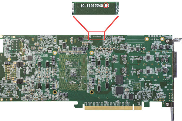
On the bottom view of the PCB, there is a seal mark for the board hardware version.
As shown in the figure below, if the letter inside the red circle is "B", it means that the PCB version is Rev.B.
Board Revision Details
Rev. A to Rev. B
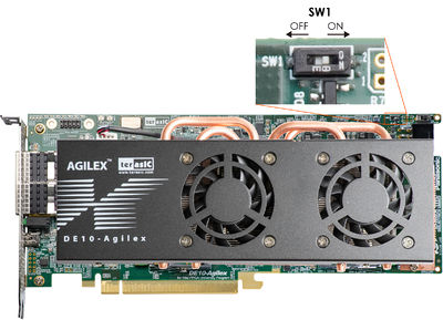
- Add Force External Power Switch (SW1) to Enable/Disable External Power Requirement when connected to the HOST PC.
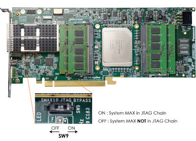
- Add System MAX10 Jtag bypass switch (SW9) for increase JTAG sacn speed.
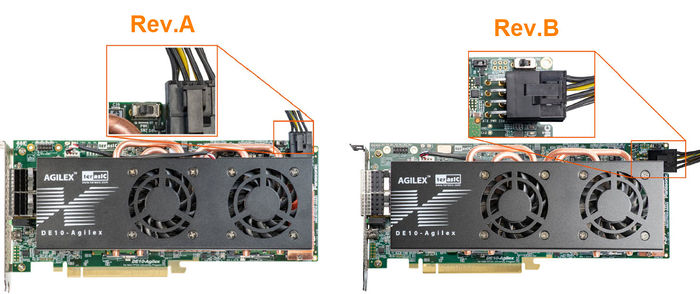
- Modify the direction of the external power connector.
- Remove DDR4 Clock Source Switch (SW5) and change the DDR4 source clock oscillator (Y2) from dual clock OSC (166.667/300.0MHz) to 33.333Mhz OSC.
- Modify the reference clock source(Y1) of the SI5340 clock generator(U13) to TCXO to increase the quality of the QSFPDD reference clock.
- Improve the core power chip(U15, VCC_CORE) from LT4680(rev.A) to LT4700(rev.B) , the power can be improve from 60A to 100A
- Rev.B board add a 30.72Mhz OCXO(U161) but it is not installed, reserved for CPRI application.
- Pin Assignment change.
| Net Name | Rev.A Pin Assignment | Rev.B Pin Assignment |
|---|---|---|
| PCIE_SMBCLK | F59 | G50 |
| PCIE_CLKREQ_n | J58 | F55 |
| PCIE_WAKE_n | G58 | J50 |
| DDR4B_SDA | H57 | B19 |
| GPIO_CLK0 | CU24 | DA22 |
| GPIO_P0 | DA22 | CY21 |
| INFO_SPI_MISO | CY21 | CU26 |


