PCA3 User Manual
From Terasic Wiki
(→Chapter 2 Architecture) |
|||
| Line 20: | Line 20: | ||
=Chapter 2 Architecture= | =Chapter 2 Architecture= | ||
This chapter provides information about architecture and block diagram of the PCA3 board. | This chapter provides information about architecture and block diagram of the PCA3 board. | ||
| + | |||
| + | ==Layout and Components== | ||
| + | The picture of the Terasic PCIe x4 Cable Adapter (PCA3) is shown in Figure 2-1 and Figure 2-2. It depicts the layout of the board and indicates the locations of the connectors and key components. | ||
| + | :::[[File:PCA3 top view.jpg|350px]]<br/> | ||
| + | :::Figure 2-1 The PCA3 Card PCB and Component Diagram (top view)<br/> | ||
| + | |||
| + | :::[[File:PCA3 bottom view.jpg|350px]]<br/> | ||
| + | :::Figure 2-2 The PCA3 Card PCB and Component Diagram (bottom view)<br/> | ||
| + | |||
| + | ==Block Diagram of the PCA3 Board== | ||
| + | Figure 2-3 shows the block diagram of the PCA3 card.<br/> | ||
| + | :::[[File:Block Diagram of PCA3.jpg|550px]]<br/> | ||
| + | :::::::::Figure 2-3 Block Diagram of PCA3 | ||
Revision as of 15:19, 20 October 2017
Contents |
Chapter 1 Introduction
The Terasic PCIe x4 Cable Adapter (PCA3) is used to connect a PCIe upstream slot with downstream target board via PCIe x4 cable, supporting PCIe x4 & x1 lanes. The PCA3 can provide programmable equalization, amplification, and de-emphasis for PCIe transceiver signal by using 8 select bits. It is also available to optimize performance over a variety of physical mediums by reducing Inter-symbol interference.
Features
Figure 1-1 shows a photograph of the PCA3 card.
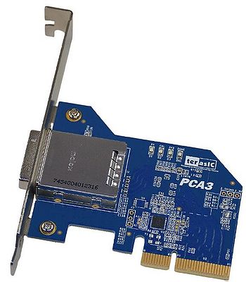
- Figure 1-1 Exterior View
- Figure 1-1 Exterior View

The key features of the card are listed below:
- Up to 8.0Gbps PCIe 3.0 Serial Re-Driver
- PCIe x4 Gen 3
- Adjustable receiver equalization
- Adjustable transmitter amplitude and de-emphasis
Getting Help
Here is information of how to get help if you encounter any problem:
Terasic Technologies
- Tel: +886-3-550-8800
- Email: support@terasic.com.cn
Chapter 2 Architecture
This chapter provides information about architecture and block diagram of the PCA3 board.
Layout and Components
The picture of the Terasic PCIe x4 Cable Adapter (PCA3) is shown in Figure 2-1 and Figure 2-2. It depicts the layout of the board and indicates the locations of the connectors and key components.
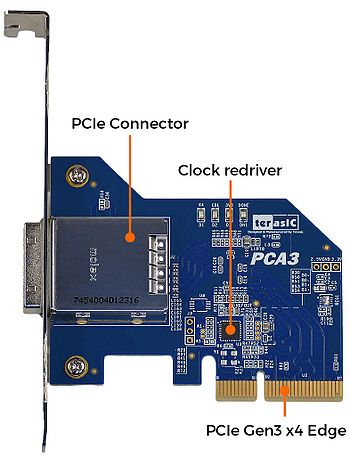
- Figure 2-1 The PCA3 Card PCB and Component Diagram (top view)

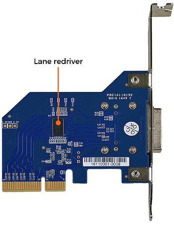
- Figure 2-2 The PCA3 Card PCB and Component Diagram (bottom view)

Block Diagram of the PCA3 Board
Figure 2-3 shows the block diagram of the PCA3 card.
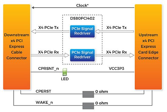
- Figure 2-3 Block Diagram of PCA3
