The Altera®
Cyclone®
V GT FPGA Development Kit can be used to prototype Cyclone®
V GT FPGA or Cyclone®
V GX FPGA applications. It offers a quick and simple way to develop low-cost and low-power FPGA system-level designs and achieve rapid results. This kit supports a myriad of functionalities such as:
•FPGA prototyping
•FPGA power measurement
•Transceiver I/O performance up to 5.0 Gbps
•PCI Express®
(PCIe®
) Gen2 x4 (at 5.0 Gbps per lane)
•Endpoint or rootport support
{page title=产品规格}}
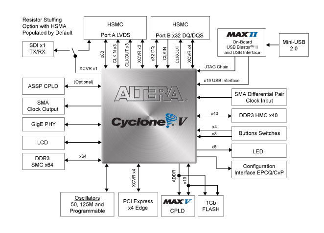
FPGA Device
- Configuration and Debug
- Quad Serial Configuration device – EPCQ256 on FPGA
- On-Board USB Blaster (Normal Type-B USB connector)
- JTAG and AS mode configuration supported
Configuration
- Communication
- Embedded USB-Blaster II (JTAG)
- Fast Passive Parallel (PFL)
- Altera EPCQ—EPCQ256SI16N (Quad Serial Configuration
Memory Device
- 384 MB x40 hard memory controller (HMC) DDR3 SDRAM with error correction code (ECC)
- 512 MB x64 soft memory controller (SMC) DDR3 SDRAM
- 1 Gb x16 sync flash
Standard communication ports
- PCIe x4 edge connector
- Gigabit Ethernet (GbE)
- One SMA clock output
- Two universal high-speed mezzanine card (HSMC) connectors, each with four high-speed serial transciever channels
- One serial digital interface (SDI) channel —1 SMB for RX and 1 SMB for TX
- Channel shared with HSMA via resistor stuffing option
Push buttons, DIP switches, and LEDs
Clocking
- Programmable clock generator for FPGA reference clock input
- 125 MHz LVDS oscillator for FPGA reference clock input
- 148.5/148.35 MHz LVDS VCXO for FPGA reference clock input
- 50 MHz single-ended oscillator for FPGA and MAX V CPLD clock input
- 100 MHz single-ended oscillator for MAX V CPLD configuration clock input
- SMA input (LVPECL)
Power
- Laptop DC Input 14 – 20 V adapter
- PCIe edge connector
System monitoring circuit
- Power (Voltage, Current, Wattage)
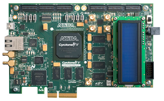
Mechanical
- PCIe card standard size (4.376" x 6.600")
Block Diagram