F2G User Manual
From Terasic Wiki
(→2-6 Pin out of the FMC connector) |
(→2-6 Pin out of the FMC connector) |
||
| Line 1,427: | Line 1,427: | ||
==2-6 Pin out of the FMC connector == | ==2-6 Pin out of the FMC connector == | ||
| - | Table 2- | + | Table 2-9 gives the pin out of the FMC connector. |
| - | <div style="text-align:center;"> '''Table | + | <div style="text-align:center;"> '''Table 2‑9 pin out of the FMC connector'''</div> |
Revision as of 16:01, 20 May 2020
Contents |
Chpater1 Introduction
The F2G board is designed to convert a FPGA Mezzanine Card(FMC) or FPGA Mezzanine Card Plus(FMC+) interface to four 2x20pin expansion prototype(GPIO) headers, which are compatible with the expansion headers of the Terasic DE-Series board(Such as DE2-115/DE10-Standard). Users can connect up to four GPIO headers onto a FMC-interfaced host board via a F2G board.
1-1 Kit Contents
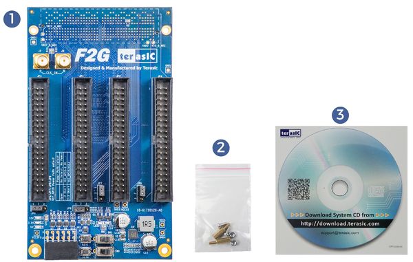
Figure 1-1 shows a photograph of the F2G package.
- F2G Card
- Screw & Copper Pillar Pakage
- CD Download Guide
1-2 Features
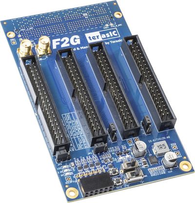
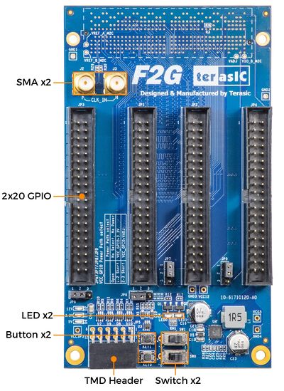
Figure 1-2 shows the photo of a F2G board. The important functions of the F2G are listed below:
- FMC High-Pin Count Interface
- I/O standard follows the definition of the mainboard without level shift
- Vcc power supply is 3.3V or adjustable according to the mainboard
- Four 2x20 GPIO Headers
- 2x6 TMD Header
- SMA Clock Input
- Button x2
- Switch x2
- LED x2
1-3 Layout and Components
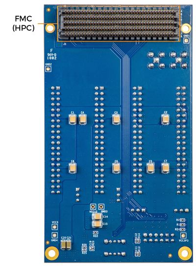
This section presents the features and design characteristics of the board. A photograph of the board is shown in Figure 1-3 and Figure 1-4. It depicts the layout of the board and indicates the location of the connectors and key components.
| Figure 1‑3 Top view of the F2G board | Figure 1‑4 Bottom view of the F2G board |
|---|---|
| 
|
1-4 Block Diagram
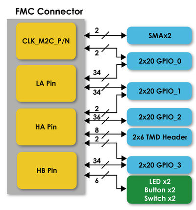
Figure 1-5 gives the block diagram of the board. According to the FMC Vita 57 specification, the FMC connector can be divided into two specifications by I/O pin numbers: high pin count and low pin count. Therefore, in the figure, we list 3 groups I/O pin in the FMC connector such as LA, HA and HB. Pins with a L prefix (LA) shall have connector contacts populated in the low-pin and high-pin count connectors.
Pins with a H prefix (HA and HB) shall have connector contacts populated only in the high-pin count connector. This will allow users to understand which F2G board interfaces can be used for their FPGA maina board.
1-5 Mechanical Specifications
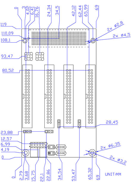
Figure 1-6 is the Mechanical Layout of F2G board.
1-6 Assemble F2G card with FPGA Main board
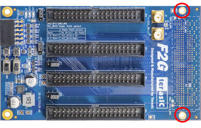
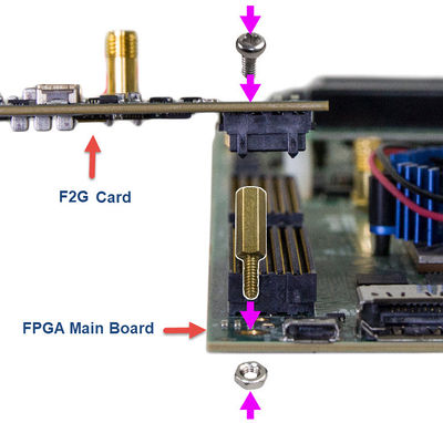
In order to make the F2G card and the FMC connector on the FMC card with more secure hookup, the FMC side of the F2G card has reserved two screw holes, as shown in Figure 1-7. Users can use the screws, copper pillars, and nuts that come with the F2G, to secure the F2G on the FPGA main board, as shown in Figure 1-8. Because transceiver is mostly used for high-speed transmission applications, we strongly recommend that users use the screws to secure the connection between the FPGA main board and the F2G card.
1-6 Getting Help
Contact us via the following methods for further technical assistance:
- Terasic Inc.9F, No.176, Sec.2, Gongdao 5th Rd, East Dist, Hsinchu City, Taiwan 300-70
- Email : support@terasic.com
- Web : www.terasic.com
Chpater 2 Board Components
This chapter provides instructions to use the board and the peripherals description.
2-1 2x20 GPIO Headers
The 2x20 GPIO header is the most important interface on the F2G board. Most of the pins on the GPIO header is directly connected to the FMC connector, allowing users to convert the FPGA I/O on the main board from FMC connector to 2.54mm GPIO header pin, which is more convenient to develop and debug.
Pin Out Of the GPIO Header
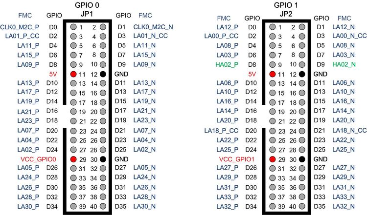
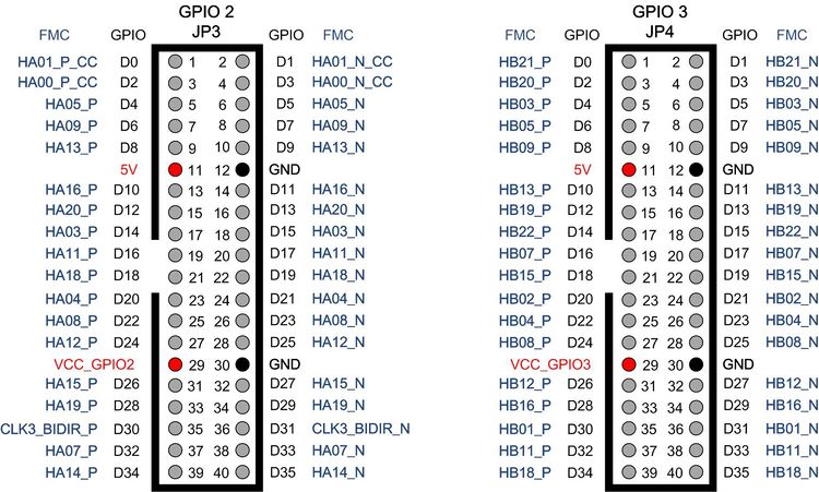
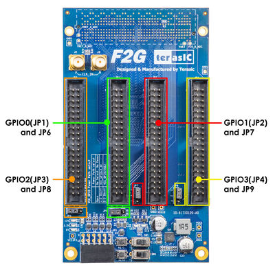
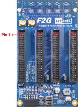
There are four 2x20 GPIO headers on the F2G board(See Figure 2-1a). Figure 2-1b shows the Pin 1 of the GPIO headers. The pin distribution and power of each GPIO header (See Figure 2-2 and Figure 2-3)is almost the same as the GPIO of Teraic DE series board. Each GPIO header can provide 36 user I / O and two sets of power supply and ground pin.
Only on pin 29: Power pin is a little different. On the F2G board, user can choose to provide 3.3V or VADJ (from maina board through FMC) via 3-pin header. For example, pin 29 on GPIO0 is VCC_GPIO0, and this power is controlled by JP6. If pin1 and pin2 of JP6 are short-circuited, then VCC_GPIO0 will be 3.3V. If short Pin 2 and Pin3, VCC_GPIO0 will be VADJ. The default setting of all the 3-pin header is short pin 1 and 2, i.e. 3.3V is provided. The control header corresponding to each GPIO header is shown in Table 2-1.
| Figure 2‑1a GPIO and 3-pin headers | Figure 2‑1b Pin 1 of the GPIO headers |
|---|---|
| 
|
| 3-Pin Header for VCCIO_GPIO | GPIO Header |
| JP6 | GPIO0(JP1) |
| JP7 | GPIO1(JP2) |
| JP8 | GPIO2(JP3) |
| JP9 | GPIO3(JP4) |
I/O standard of the GPIO headers
Because the GPIO header is directly connected to the I/O of the FMC connector and has not been converted by any level translator. Therefore, the I / O standard of the GPIO header depends on the voltage settings on the FPGA maina board. So, before using or connecting any circuit to the GPIO header, please check whether the logic level matches the FPGA main board.
Support status for HPC and LPC of FMC connector
The number of pin I / O of the FMC connector is divided into two specifications: high pin count(HPC) and low pin count(LPC). As shown in Figure 1-5, If the FMC connector on the user's main board is low pin count, type, you can only use the two headers : GPIO_0 and GPIO1 on F2G board. It should be noted that there are two I / O(GPIO_1_D8 and GPIO_1_D9) on GPIO_1 that are connected to the pin group of high pin count, so these two I/O will also be unavailable(See Figure 2-2). If the user's main board is HPC type, the four GPIO headers on F2G board are all can be used.
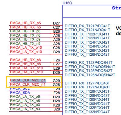
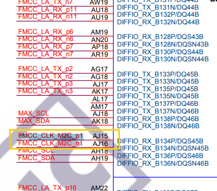
In addition, it should be noted that many FPGA maina board may place some terminal resistors on the FMC I/O for differential I/O standard or clock I/O. To use the GPIO header pin on F2G, you may need to remove these resistors between the I/O first to avoid interfere with each other. For example, GPIO_0_D0/GPIO_0_D1 on GPIO_0 header are connected to the CLK0_M2C_P/CLK0_M2C_N pin of the FMC connector. On many FPGA main boards, a terminal resistor may be reserved for this pair of I/O. If users want to use both GPIO_0_D0 and GPIO_0_D1, you may need to check and remove the resistance on the main board first to avoid the two I/O interfere with each other. for more examples, please refer to Section 2-5.
Pin Mappings for GPIO and FMC
Table 2-2, Table 2-3,Table 2-4 and Table 2-5 list the list each GPIO header pin number and signal name and the connected FMC pin.
| GPIO Pin No. | GPIO Pin Signal Name | FMC Pin No. | FMC Pin Signal Name | I/O Standard |
| 1 | GPIO_0_D0 | H4 | CLK0_M2C_P | VADJ (Depend on User's main board) |
| 2 | GPIO_0_D1 | H5 | CLK0_M2C_N | |
| 3 | GPIO_0_D2 | D8 | LA01_P_CC | |
| 4 | GPIO_0_D3 | D9 | LA01_N_CC | |
| 5 | GPIO_0_D4 | H16 | LA11_P | |
| 6 | GPIO_0_D5 | H17 | LA11_N | |
| 7 | GPIO_0_D6 | H19 | LA15_P | |
| 8 | GPIO_0_D7 | H20 | LA15_N | |
| 9 | GPIO_0_D8 | D14 | LA09_P | |
| 10 | GPIO_0_D9 | D15 | LA09_N | |
| 11 | VCC5 | -- | -- | 5V |
| 12 | GND | -- | -- | Ground |
| 13 | GPIO_0_D10 | D17 | LA13_P | VADJ (Depend on User's main board) |
| 14 | GPIO_0_D11 | D18 | LA13_N | |
| 15 | GPIO_0_D12 | D20 | LA17_P_CC | |
| 16 | GPIO_0_D13 | D21 | LA17_N_CC | |
| 17 | GPIO_0_D14 | H22 | LA19_P | |
| 18 | GPIO_0_D15 | H23 | LA19_N | |
| 19 | GPIO_0_D16 | H25 | LA21_P | |
| 20 | GPIO_0_D17 | H26 | LA21_N | |
| 21 | GPIO_0_D18 | D23 | LA23_P | |
| 22 | GPIO_0_D19 | D24 | LA23_N | |
| 23 | GPIO_0_D20 | H13 | LA07_P | |
| 24 | GPIO_0_D21 | H14 | LA07_N | |
| 25 | GPIO_0_D22 | H10 | LA04_P | |
| 26 | GPIO_0_D23 | H11 | LA04_N | |
| 27 | GPIO_0_D24 | H7 | LA02_P | |
| 28 | GPIO_0_D25 | H8 | LA02_N | |
| 29 | VCC_GPIO0(*1) | -- | -- | 3.3V or VADJ |
| 30 | GND | -- | -- | Ground |
| 31 | GPIO_0_D26 | D11 | LA05_P | VADJ (Depend on User's main board) |
| 32 | GPIO_0_D27 | D12 | LA05_N | |
| 33 | GPIO_0_D28 | H28 | LA24_P | |
| 34 | GPIO_0_D29 | H29 | LA24_N | |
| 35 | GPIO_0_D30 | D26 | LA26_P | |
| 36 | GPIO_0_D31 | D27 | LA26_N | |
| 37 | GPIO_0_D32 | H31 | LA28_P | |
| 38 | GPIO_0_D33 | H32 | LA28_N | |
| 39 | GPIO_0_D34 | H34 | LA30_P | |
| 40 | GPIO_0_D35 | H35 | LA30_N |
| GPIO Pin No. | GPIO Pin Signal Name | FMC Pin No. | FMC Pin Signal Name | I/O Standard |
| 1 | GPIO_1_D0 | G15 | LA12_P | VADJ (Depend on User's main board) |
| 2 | GPIO_1_D1 | G16 | LA12_N | |
| 3 | GPIO_1_D2 | G6 | LA00_P_CC | |
| 4 | GPIO_1_D3 | G7 | LA00_N_CC | |
| 5 | GPIO_1_D4 | G12 | LA08_P | |
| 6 | GPIO_1_D5 | G13 | LA08_N | |
| 7 | GPIO_1_D6 | G9 | LA03_P | |
| 8 | GPIO_1_D7 | G10 | LA03_N | |
| 9 | GPIO_1_D8 | K7 | HA02_P | |
| 10 | GPIO_1_D9 | K8 | HA02_N | |
| 11 | VCC5 | -- | -- | 5V |
| 12 | GND | -- | -- | Ground |
| 13 | GPIO_1_D10 | C10 | LA06_P | VADJ (Depend on User's main board) |
| 14 | GPIO_1_D11 | C11 | LA06_N | |
| 15 | GPIO_1_D12 | C14 | LA10_P | |
| 16 | GPIO_1_D13 | C15 | LA10_N | |
| 17 | GPIO_1_D14 | G18 | LA16_P | |
| 18 | GPIO_1_D15 | G19 | LA16_N | |
| 19 | GPIO_1_D16 | C18 | LA14_P | |
| 20 | GPIO_1_D17 | C19 | LA14_N | |
| 21 | GPIO_1_D18 | G21 | LA20_P | |
| 22 | GPIO_1_D19 | G22 | LA20_N | |
| 23 | GPIO_1_D20 | C22 | LA18_P_CC | |
| 24 | GPIO_1_D21 | C23 | LA18_N_CC | |
| 25 | GPIO_1_D22 | G24 | LA22_P | |
| 26 | GPIO_1_D23 | G25 | LA22_N | |
| 27 | GPIO_1_D24 | G27 | LA25_P | |
| 28 | GPIO_1_D25 | G28 | LA25_N | |
| 29 | VCC_GPIO1(*1) | -- | -- | 3.3V or VADJ |
| 30 | GND | -- | -- | Ground |
| 31 | GPIO_1_D26 | C26 | LA27_P | VADJ (Depend on User's main board) |
| 32 | GPIO_1_D27 | C27 | LA27_N | |
| 33 | GPIO_1_D28 | G30 | LA29_P | |
| 34 | GPIO_1_D29 | G31 | LA29_N | |
| 35 | GPIO_1_D30 | G33 | LA31_P | |
| 36 | GPIO_1_D31 | G34 | LA31_N | |
| 37 | GPIO_1_D32 | G36 | LA33_P | |
| 38 | GPIO_1_D33 | G37 | LA33_N | |
| 39 | GPIO_1_D34 | H37 | LA32_P | |
| 40 | GPIO_1_D35 | H38 | LA32_N |
| GPIO Pin No. | GPIO Pin Signal Name | FMC Pin No. | FMC Pin Signal Name | I/O Standard | |
| 1 | GPIO_2_D0 | E2 | HA01_P_CC | VADJ (Depend on User's main board) | |
| 2 | GPIO_2_D1 | E3 | HA01_N_CC | ||
| 3 | GPIO_2_D2 | F4 | HA00_P_CC | ||
| 4 | GPIO_2_D3 | F5 | HA00_N_CC | ||
| 5 | GPIO_2_D4 | E6 | HA05_P | ||
| 6 | GPIO_2_D5 | E7 | HA05_N | ||
| 7 | GPIO_2_D6 | E9 | HA09_P | ||
| 8 | GPIO_2_D7 | E10 | HA09_N | ||
| 9 | GPIO_2_D8 | E12 | HA13_P | ||
| 10 | GPIO_2_D9 | E13 | HA13_N | ||
| 11 | VCC5 | -- | -- | 5V | |
| 12 | GND | -- | -- | Ground | |
| 13 | GPIO_2_D10 | E15 | HA16_P | VADJ (Depend on User's main board) | |
| 14 | GPIO_2_D11 | E16 | HA16_N | ||
| 15 | GPIO_2_D12 | E18 | HA20_P | ||
| 16 | GPIO_2_D13 | E19 | HA20_N | ||
| 17 | GPIO_2_D14 | J6 | HA03_P | ||
| 18 | GPIO_2_D15 | J7 | HA03_N | ||
| 19 | GPIO_2_D16 | J12 | HA11_P | ||
| 20 | GPIO_2_D17 | J13 | HA11_N | ||
| 21 | GPIO_2_D18 | J18 | HA18_P | ||
| 22 | GPIO_2_D19 | J19 | HA18_N | ||
| 23 | GPIO_2_D20 | F7 | HA04_P | ||
| 24 | GPIO_2_D21 | F8 | HA04_N | ||
| 25 | GPIO_2_D22 | F10 | HA08_P | ||
| 26 | GPIO_2_D23 | F11 | HA08_N | ||
| 27 | GPIO_2_D24 | F13 | HA12_P | ||
| 28 | GPIO_2_D25 | F14 | HA12_N | ||
| 29 | VCC_GPIO2(*1) | -- | -- | 3.3V or VADJ | |
| 30 | GND | -- | -- | Ground | |
| 31 | GPIO_2_D26 | F16 | HA15_P | VADJ (Depend on User's main board) | |
| 32 | GPIO_2_D27 | F17 | HA15_N | ||
| 33 | GPIO_2_D28 | F19 | HA19_P | ||
| 34 | GPIO_2_D29 | F20 | HA19_N | ||
| 35 | GPIO_2_D30 | J2 | CLK3_BIDIR_P | ||
| 36 | GPIO_2_D31 | J3 | CLK3_BIDIR_N | ||
| 37 | GPIO_2_D32 | J9 | HA07_P | ||
| 38 | GPIO_2_D33 | J10 | HA07_N | ||
| 39 | GPIO_2_D34 | J15 | HA14_P | ||
| 40 | GPIO_2_D35 | J16 | HA14_N | ||
| GPIO Pin No. | GPIO Pin Signal Name | FMC Pin No. | FMC Pin Signal Name | I/O Standard | |
| 1 | GPIO_3_D0 | E36 | HB21_P | VADJ (Depend on User's main board) | |
| 2 | GPIO_3_D1 | E37 | HB21_N | ||
| 3 | GPIO_3_D2 | F37 | HB20_P | ||
| 4 | GPIO_3_D3 | F38 | HB20_N | ||
| 5 | GPIO_3_D4 | E21 | HB03_P | ||
| 6 | GPIO_3_D5 | E22 | HB03_N | ||
| 7 | GPIO_3_D6 | E24 | HB05_P | ||
| 8 | GPIO_3_D7 | E25 | HB05_N | ||
| 9 | GPIO_3_D8 | E27 | HB09_P | ||
| 10 | GPIO_3_D9 | E28 | HB09_N | ||
| 11 | VCC5 | -- | -- | 5V | |
| 12 | GND | -- | -- | Ground | |
| 13 | GPIO_3_D10 | E30 | HB13_P | VADJ (Depend on User's main board) | |
| 14 | GPIO_3_D11 | E31 | HB13_N | ||
| 15 | GPIO_3_D12 | E33 | HB19_P | ||
| 16 | GPIO_3_D13 | E34 | HB19_N | ||
| 17 | GPIO_3_D14 | J21 | HA22_P | ||
| 18 | GPIO_3_D15 | J22 | HA22_N | ||
| 19 | GPIO_3_D16 | J27 | HB07_P | ||
| 20 | GPIO_3_D17 | J28 | HB07_N | ||
| 21 | GPIO_3_D18 | J33 | HB15_P | ||
| 22 | GPIO_3_D19 | J34 | HB15_N | ||
| 23 | GPIO_3_D20 | F22 | HB02_P | ||
| 24 | GPIO_3_D21 | F23 | HB02_N | ||
| 25 | GPIO_3_D22 | F25 | HB04_P | ||
| 26 | GPIO_3_D23 | F26 | HB04_N | ||
| 27 | GPIO_3_D24 | F28 | HB08_P | ||
| 28 | GPIO_3_D25 | F29 | HB08_N | ||
| 29 | VCC_GPIO3(*1) | -- | -- | 3.3V or VADJ | |
| 30 | GND | -- | -- | Ground | |
| 31 | GPIO_3_D26 | F31 | HB12_P | VADJ (Depend on User's main board) | |
| 32 | GPIO_3_D27 | F32 | HB12_N | ||
| 33 | GPIO_3_D28 | F34 | HB16_P | ||
| 34 | GPIO_3_D29 | F35 | HB16_N | ||
| 35 | GPIO_3_D30 | J24 | HB01_P | ||
| 36 | GPIO_3_D31 | J25 | HB01_N | ||
| 37 | GPIO_3_D32 | J30 | HB11_P | ||
| 38 | GPIO_3_D33 | J31 | HB11_N | ||
| 39 | GPIO_3_D34 | J36 | HB18_P | ||
| 40 | GPIO_3_D35 | J37 | HB18_N | ||
(*1) : VCCIO_GPIO0/VCCIO_GPIO1/VCCIO_GPIO2/VCCIO_GPIO3 is determined by 3-pin headers for 3.3V or VADJ, please refer to section: Pin Out Of the GPIO Header for details
2-2 2x6 TMD Headers
The F2G board has one 2x6 TMD (Terasic Mini Digital) expansion header. The TMD header has 8 digital GPIO user pins connected to the FMC connector directly, two 3.3V power pins and two ground pins. There are two Transient Voltage Suppressor diode arrays used to implement ESD protection for 8 GPIO user pins.
Also, like the 2x20 GPIO header, the supported I/O standard of the TMD header is also determined by the settings on the FPGA main board. Users need to pay attention to whether the circuit connected to the TMD header matches the I/O standard on the main board. In addition, due to the TMD header is connected to the HA pin group on the FMC connector, so the TMD header can only be used on the FPGA main board which support the high pin count FMC connector.
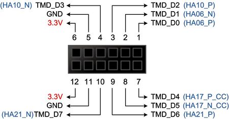
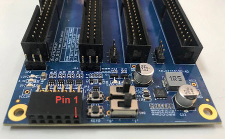
Figure 2-4 shows the pin-outs of the TMD header and Figure 2-5 indicates the pin 1 of the TMD header. Table 2-6 gives the pin mappings of the TMD header.
| TMD Pin No. | TMD Pin Signal Name | FMC Pin No. | FMC Pin Signal Name | I/O Standard |
| 1 | TMD_D0 | K10 | HA06_P | VADJ (Depend on User's main board) |
| 2 | TMD_D1 | K11 | HA06_N | |
| 3 | TMD_D2 | K13 | HA10_P | |
| 4 | TMD_D3 | K14 | HA10_N | |
| 5 | GND | -- | -- | Ground |
| 6 | 3.3V | -- | -- | 3.3V |
| 7 | TMD_D4 | K16 | HA17_P_CC | VADJ (Depend on User's main board) |
| 8 | TMD_D5 | K17 | HA17_N_CC | |
| 9 | TMD_D6 | K19 | HA21_P | |
| 10 | TMD_D7 | K20 | HA21_N | |
| 11 | GND | -- | -- | Ground |
| 12 | 3.3V | -- | -- | 3.3V |
2-3 Push-buttons, Switches and LEDs
- User-Defined Push-buttons
- The board includes two user defined push-buttons that allow users to interact with the FPGA device on the FPGA main board. Each of these switches is debounced using a Schmitt Trigger circuit. A Schmitt trigger feature introduces hysteresis to the input signal for improved noise immunity, especially for signal with slow edge rate and act as switch debounce for the push-buttons connected. Table 2-7 list the pin assignment of user push-buttons.
| Push-button Signal Name | FMC Pin No. | FMC Pin Signal Name |
| KEY1 | K34 | HB14_P |
| KEY2 | K35 | HB14_N |
- User-Defined Dip Switch
- There are 2 position dip switches connected to FMC connector. These switches are used as level-sensitive data inputs to a circuit. Every one of the switches is connected directly and individually to a pin on the FMC connector. Table 2-8 list the pin assignments of the user switches.
| Dip Switch Signal Name | FMC Pin No. | FMC Pin Signal Name |
| SW0 | K37 | HB17_P_CC |
| SW1 | K38 | HB17_N_CC |
- User-Defined LEDs
- There are also 2 user-controllable LEDs connected to FMC connector on the board. Each LED is driven by FMC connector; driving its associated pin to a high logic level turns the LED on, and driving the pin low turns it off. Table 2-9 list the pin assignment of user LEDs.
| LED Signal Name | FMC Pin No. | FMC Pin Signal Name |
| LED0 | K22 | HB23_P |
| LED1 | K23 | HB23_N |
Note that user I/Os such as Push-buttons, Switches and LEDs are connected to the FMC connector's HB group pin, so if the FMC connector of user's FPGA main board is a low pin count type, these interfaces will not be available.
2-4 SMA connectors for clock input
A pair of SMA connectors are provided on the F2G board so that users can input differenteantial or single-end clock into the FPGA main board through these pair of connectors. It should be noted that the SMA connector and FMC connector are directly connected, so the input clock I/O Standard needs to match the settings of the main board. Table 2-10 give the pin mapping of the SMA connectors.
| SMA conenctor | SMA Signal Name | FMC Pin No. | FMC Pin Signal Name |
| J2 | SMA_CLK_p | G2 | CLK1_M2C_P |
| J3 | SMA_CLK_n | G3 | CLK1_M2C_N |
2-5 Support status for Terasic's FMC main board
This section will introduce the support status and important notes when using F2G board on the Terasic FPGA main board with FMC connector. As shown in Table 2-8, we list which interface on the F2G board can be used when the F2G board is connected to Terasic's TR5 (Stratix V), HAN Pilot Platform (Arria 10) and Apollo S10 (Stratix 10). Also it will list some notes for some special pins.
| GOIO_0 | GOIO_1 | GOIO_2 | GOIO_3 | TMD | SMA | LED/Button/Switch | ||
| TR5 | FMC-A
(HPC)
| Support | Support
*Note2
| Support
*Note3
| Support | Support | Can't be used for clock input
*Note4 | Support |
| FMC-B
(LPC) | Support
*Note1
| Support
(Except GPIO_1_D8 and GPIO_1_D9)
*Note2
| Not Support | Not Support | Not Support | Support | Not Support | |
| FMC-C
(LPC) | Support | Support
(Except GPIO_1_D8 and GPIO_1_D9)
*Note2
| Not Support | Not Support | Not Support | Can't be used for clock input
*Note4 | Not Support | |
| FMC-D
(HPC) | Support | Support
*Note2
| Support
*Note3
| Support | Support | Support | Support | |
| HAN | FMC
(HPC)
| Support | Support | Support | Support | Support | Support | Support |
| Apollo S10 SoM | FMC
(HPC) | Support | Support | Support | Support | Support | Support | Support |
| FMC+ | Support | Support | Support | Support | Support | Support | Support | |
*Note1 :When the F2G board is connected to the FMC-B connector of TR5 board, Pin GPIO_0_D0 and GPIO_0_D1 on GPIO0 are connected to the TR5 via FMC connector, a parallel resistor R274 on the TR5 will be connected to these two signal. It is recommended to remove this resistor to prevent GPIO_0_D0 and GPIO_0_D1 from interfering with each other.
*Note2 :When the F2G board is connected to the FMC-A connector of TR5 board, Pin GPIO_1_D2 and GPIO_1_D3 on GPIO1 are connected to the TR5 via FMC connector, a parallel resistor R280 on the TR5 will be connected to these two signal. It is recommended to remove this resistor to prevent GPIO_1_D2 and GPIO_1_D3 from interfering with each other.
Similarly, when the F2G is connected to TR5's FMC-B connector, R294 resistor needs to be removed; when the F2G is connected to TR5's FMC-C connector, R294 resistor needs to be removed; when the F2G is connected to TR5's FMC-D connector, R355 resistor needs to be removed to avoid GPIO_1_D2 and GPIO_1_D3 signal interfering with each other.
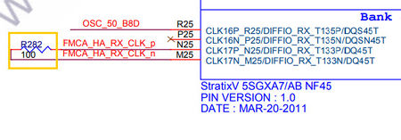
*Note3 :When the F2G board is connected to the FMC-A connector of TR5 board, Pin GPIO_2_D0 and GPIO_2_D1 on GPIO2 are connected to the TR5 via FMC connector, a parallel resistor R282 on the TR5 will be connected to these two signal. It is recommended to remove this resistor to prevent GPIO_2_D0 and GPIO_2_D1 from interfering with each other.
Similarly, when the F2G is connected to TR5's FMC-D connector, R279 resistor needs to be removed;
*Note4 : The SMA connectors on the F2G board is mainly designed to input the clock to the FPGA main board, but not every FPGA main board connects this pair of clock signal to the dedicated clock pin for FPGA. On TR5 board, these two clock signal on the FMC connectors FMC-A and FMC-C don't be connected to the dedicated clock pins. If users connect F2G to these two FMC connectors, they can only use this pair of SMA connector as ordinary I/O.
2-6 Pin out of the FMC connector
Table 2-9 gives the pin out of the FMC connector.
| K | J | H | G | F | E | D | C | B | A | |
| 1 | FMC_VREFB | GND | FMC_VREFA | GND | NC | GND | NC | GND | NC | GND |
| 2 | GND | GPIO_2_D30 | NC | SMA_CLK_P | GND | GPIO_2_D0 | GND | NC | GND | NC |
| 3 | GND | GPIO_2_D31 | GND | SMA_CLK_N | GND | GPIO_2_D1 | GND | NC | GND | NC |
| 4 | NC | GND | GPIO_0_D0 | GND | GPIO_2_D2 | GND | NC | GND | NC | GND |
| 5 | NC | GND | GPIO_0_D1 | GND | GPIO_2_D3 | GND | NC | GND | NC | GND |
| 6 | GND | GPIO_2_D14 | GND | GPIO_1_D2 | GND | GPIO_2_D4 | GND | NC | GND | NC |
| 7 | GPIO_1_D8 | GPIO_2_D15 | GPIO_0_D24 | GPIO_1_D3 | GPIO_2_D20 | GPIO_2_D5 | GND | NC | GND | NC |
| 8 | GPIO_1_D9 | GND | GPIO_0_D25 | GND | GPIO_2_D21 | GND | GPIO_0_D2 | GND | NC | GND |
| 9 | GND | GPIO_2_D32 | GND | GPIO_1_D6 | GND | GPIO_2_D6 | GPIO_0_D3 | GND | NC | GND |
| 10 | TMD_D0 | GPIO_2_D33 | GPIO_0_D22 | GPIO_1_D7 | GPIO_2_D22 | GPIO_2_D7 | GND | GPIO_1_D10 | GND | NC |
| 11 | TMD_D1 | GND | GPIO_0_D23 | GND | GPIO_2_D23 | GND | GPIO_0_D26 | GPIO_1_D11 | GND | NC |
| 12 | GND | GPIO_2_D16 | GND | GPIO_1_D4 | GND | GPIO_2_D8 | GPIO_0_D27 | GND | NC | GND |
| 13 | TMD_D2 | GPIO_2_D17 | GPIO_0_D20 | GPIO_1_D5 | GPIO_2_D24 | GPIO_2_D9 | GND | GND | NC | GND |
| 14 | TMD_D3 | GND | GPIO_0_D21 | GND | GPIO_2_D25 | GND | GPIO_0_D8 | GPIO_1_D12 | GND | NC |
| 15 | GND | GPIO_2_D34 | GND | GPIO_1_D0 | GND | GPIO_2_D10 | GPIO_0_D9 | GPIO_1_D13 | GND | NC |
| 16 | TMD_D4 | GPIO_2_D35 | GPIO_0_D4 | GPIO_1_D1 | GPIO_2_D26 | GPIO_2_D11 | GND | GND | NC | GND |
| 17 | TMD_D5 | GND | GPIO_0_D5 | GND | GPIO_2_D27 | GND | GPIO_0_D10 | GND | NC | GND |
| 18 | GND | GPIO_2_D18 | GND | GPIO_1_D14 | GND | GPIO_2_D12 | GPIO_0_D11 | GPIO_1_D16 | GND | NC |
| 19 | TMD_D6 | GPIO_2_D19 | GPIO_0_D6 | GPIO_1_D15 | GPIO_2_D28 | GPIO_2_D13 | GND | GPIO_1_D17 | GND | NC |
| 20 | TMD_D7 | GND | GPIO_0_D7 | GND | GPIO_2_D29 | GND | GPIO_0_D12 | GND | NC | GND |
| 21 | GND | GPIO_3_D14 | GND | GPIO_1_D18 | GND | GPIO_3_D4 | GPIO_0_D13 | GND | NC | GND |
| 22 | LED0 | GPIO_3_D15 | GPIO_0_D14 | GPIO_1_D19 | GPIO_3_D20 | GPIO_3_D5 | GND | GPIO_1_D20 | GND | NC |
| 23 | LED1 | GND | GPIO_0_D15 | GND | GPIO_3_D21 | GND | GPIO_0_D18 | GPIO_1_D21 | GND | NC |
| 24 | GND | GPIO_3_D30 | GND | GPIO_1_D22 | GND | GPIO_3_D6 | GPIO_0_D19 | GND | NC | GND |
| 25 | NC | GPIO_3_D31 | GPIO_0_D16 | GPIO_1_D23 | GPIO_3_D22 | GPIO_3_D7 | GND | GND | NC | GND |
| 26 | NC | GND | GPIO_0_D17 | GND | GPIO_3_D23 | GND | GPIO_0_D30 | GPIO_1_D26 | GND | NC |
| 27 | GND | GPIO_3_D16 | GND | GPIO_1_D24 | GND | GPIO_3_D8 | GPIO_0_D31 | GPIO_1_D27 | GND | NC |
| 28 | NC | GPIO_3_D17 | GPIO_0_D28 | GPIO_1_D25 | GPIO_3_D24 | GPIO_3_D9 | GND | GND | NC | GND |
| 29 | NC | GND | GPIO_0_D29 | GND | GPIO_3_D25 | GND | NC | GND | NC | GND |
| 30 | GND | GPIO_3_D32 | GND | GPIO_1_D28 | GND | GPIO_3_D10 | NC | NC | GND | NC |
| 31 | NC | GPIO_3_D33 | GPIO_0_D32 | GPIO_1_D29 | GPIO_3_D26 | GPIO_3_D11 | NC | NC | GND | NC |
| 32 | NC | GND | GPIO_0_D33 | GND | GPIO_3_D27 | GND | VCC3P3 | GND | NC | GND |
| 33 | GND | GPIO_3_D18 | GND | GPIO_1_D30 | GND | GPIO_3_D12 | NC | GND | NC | GND |
| 34 | KEY0 | GPIO_3_D19 | GPIO_0_D34 | GPIO_1_D31 | GPIO_3_D28 | GPIO_3_D13 | NC | NC | GND | NC |
| 35 | KEY1 | GND | GPIO_0_D35 | GND | GPIO_3_D29 | GND | NC | VCC12 | GND | NC |
| 36 | GND | GPIO_3_D34 | GND | GPIO_1_D32 | GND | GPIO_3_D0 | VCC3P3 | GND | NC | GND |
| 37 | SW0 | GPIO_3_D35 | GPIO_1_D34 | GPIO_1_D33 | GPIO_3_D2 | GPIO_3_D1 | GND | VCC12 | NC | GND |
| 38 | SW1 | GND | GPIO_1_D35 | GND | GPIO_3_D3 | GND | VCC3P3 | GND | GND | NC |
| 39 | GND | VIO_B_M2C | GND | VADJ | GND | VADJ | GND | VCC3P3 | GND | NC |
| 40 | VIO_B_M2C | GND | VADJ | GND | VADJ | GND | VCC3P3 | GND | NC | GND |
