F2G User Manual
From Terasic Wiki
Contents |
Chpater1 Introduction
The F2G board is designed to convert a FPGA Mezzanine Card(FMC) or FPGA Mezzanine Card Plus(FMC+) interface to four 2x20pin expansion prototype(GPIO) connectors, which are compatible with the expansion headers of the Terasic DE-Series board(Such as DE2-115/DE10-Standard). Users can connect up to four GPIO connectors onto a FMC-interfaced host board via a F2G board.
1-1 Kit Contents
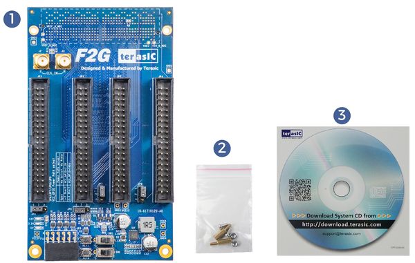
Figure 1-1 shows a photograph of the F2G package.
- F2G Card
- Screw & Copper Pillar Pakage
- CD Download Guide
1-2 Features
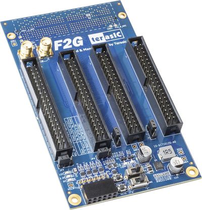
Figure 1-2 shows the photo of a F2G board. The important functions of the F2G are listed below:
- FMC High-Pin Count Interface.
- IO standard is dependent on FMC Voltage of the Mother board.
- Four 2x20 GPIO Headers.
- 2x6 TMD Header.
- SMA Clock Input.
- Button x2.
- SWtich x2.
- LED x2.
1-3 Layout and Components
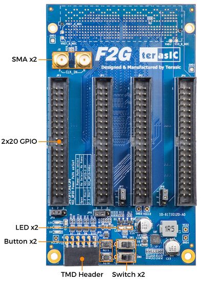
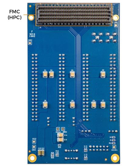
This section presents the features and design characteristics of the board. A photograph of the board is shown in Figure 1-3 and Figure 1-4 It depicts the layout of the board and indicates the location of the connectors and key components.
1-4 Block Diagram
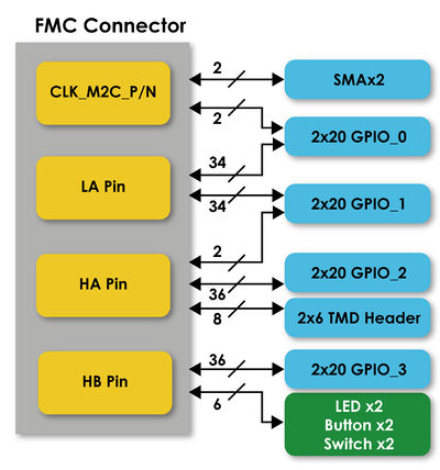
Figure 1-5 gives the block diagram of the board. According to the FMC Vita 57 specification, the FMC connector can be divided into two specifications by I/O pin numbers: high pin count and low pin count. Therefore, in the figure, we list 3 groups I/O pin in the FMC connector such as LA, HA and HB. Pins with a L prefix (LA) shall have connector contacts populated in the low-pin and high-pin count connectors.
Pins with a H prefix (HA and HB) shall have connector contacts populated only in the high-pin count connector. This will allow users to understand which F2G board interfaces can be used for their FPGA motherboard.
1-5 Mechanical Specifications
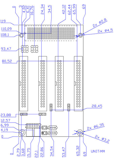
Figure 1-6 is the Mechanical Layout of F2G board.
1-6 Getting Help
Contact us via the following methods for further technical assistance:
- Terasic Inc.9F, No.176, Sec.2, Gongdao 5th Rd, East Dist, Hsinchu City, Taiwan 300-70
- Email : support@terasic.com
- Web : www.terasic.com
Chpater 2 Board Components
This chapter provides instructions to use the board and the peripherals description.
2-1 2x20 GPIO Headers
The 2x20 GPIO header is the most important interface on the F2G board. Most of the pins on the GPIO headr is directly connected to the FMC connector, allowing users to convert the FPGA I/O on the mother board from FMC connector to 2.54mm GPIO headr pin, which is more convenient to develop and debug.
There are four 2x20 GPIO headers on F2G. The pin distribution and power of each GPIO header is almost the same as the GPIO of Teraic DE series board. Only on pin 29: Power pin is a little different. On the F2G board, user can choose to provide 3.3V or VADJ from motherboard through FMC via 3-pin header.
| GPIO Pin No. | GPIO Pin Signal Name | FMC Pin No. | FMC Pin Signal Name | I/O Standard |
| 1 | GPIO_0_D0 | H4 | CLK0_M2C_P | VADJ (Depend on User's mother board) |
| 2 | GPIO_0_D1 | H5 | CLK0_M2C_N | |
| 3 | GPIO_0_D2 | D8 | LA01_P_CC | |
| 4 | GPIO_0_D3 | D9 | LA01_N_CC | |
| 5 | GPIO_0_D4 | H16 | LA11_P | |
| 6 | GPIO_0_D5 | H17 | LA11_N | |
| 7 | GPIO_0_D6 | H19 | LA15_P | |
| 8 | GPIO_0_D7 | H20 | LA15_N | |
| 9 | GPIO_0_D8 | D14 | LA09_P | |
| 10 | GPIO_0_D9 | D15 | LA09_N | |
| 11 | VCC5 | -- | -- | 5V |
| 12 | GND | -- | -- | Ground |
| 13 | GPIO_0_D10 | D17 | LA13_P | VADJ (Depend on User's mother board) |
| 14 | GPIO_0_D11 | D18 | LA13_N | |
| 15 | GPIO_0_D12 | D20 | LA17_P_CC | |
| 16 | GPIO_0_D13 | D21 | LA17_N_CC | |
| 17 | GPIO_0_D14 | H22 | LA19_P | |
| 18 | GPIO_0_D15 | H23 | LA19_N | |
| 19 | GPIO_0_D16 | H25 | LA21_P | |
| 20 | GPIO_0_D17 | H26 | LA21_N | |
| 21 | GPIO_0_D18 | D23 | LA23_P | |
| 22 | GPIO_0_D19 | D24 | LA23_N | |
| 23 | GPIO_0_D20 | H13 | LA07_P | |
| 24 | GPIO_0_D21 | H14 | LA07_N | |
| 25 | GPIO_0_D22 | H10 | LA04_P | |
| 26 | GPIO_0_D23 | H11 | LA04_N | |
| 27 | GPIO_0_D24 | H7 | LA02_P | |
| 28 | GPIO_0_D25 | H8 | LA02_N | |
| 29 | VCC_GPIO0(*1) | -- | -- | 3.3V or VADJ |
| 30 | GND | -- | -- | Ground |
| 31 | GPIO_0_D26 | D11 | LA05_P | VADJ (Depend on User's mother board) |
| 32 | GPIO_0_D27 | D12 | LA05_N | |
| 33 | GPIO_0_D28 | H28 | LA24_P | |
| 34 | GPIO_0_D29 | H29 | LA24_N | |
| 35 | GPIO_0_D30 | D26 | LA26_P | |
| 36 | GPIO_0_D31 | D27 | LA26_N | |
| 37 | GPIO_0_D32 | H31 | LA28_P | |
| 38 | GPIO_0_D33 | H32 | LA28_N | |
| 39 | GPIO_0_D34 | H34 | LA30_P | |
| 40 | GPIO_0_D35 | H35 | LA30_N |
