DE10-Advance Hardware Manual revC Chapter2 Block Diagram
From Terasic Wiki
2.2 Block Diagram of the DE10-Advanced Board
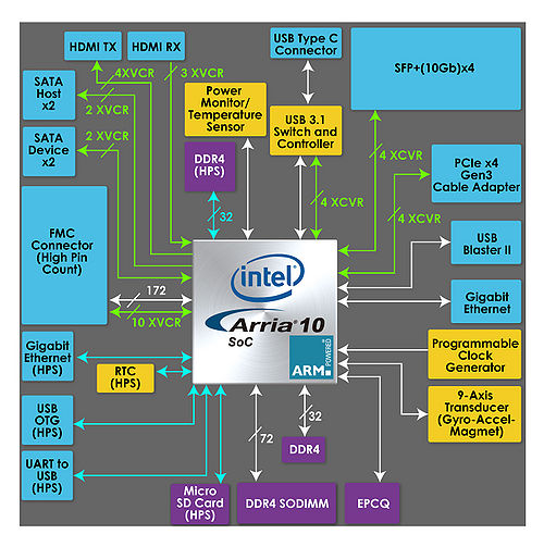
Figure 2-3 is the block diagram of the board. All the connections are established through the Arria 10 SoC FPGA device to provide maximum flexibility for users. Users can configure the FPGA to implement any system design.
- Figure 2-3 Block diagram of DE10-Advanced
Detailed information about Figure 2-3 are listed below.
- Arria 10 SoC 10AS066K3F40E2SG/10AS057K3F40E2SG FPGA
- Dual-core ARM Cortex-A9 (HPS)
- 660K programmable logic elements
- 42,660 Kbits embedded memory
- Hard memory controllers x5
- Transceivers x48(17.4 Gbps)
- 18-bit x 19-bit multipliers x3,356
- Accelerometer & Gyroscope Device MPU9250
- Configuration
- EPCQ1024L Serial Configuration Device
- Onboard USB-Blaster II (Mini-B USB connector)
- Memory Device
- On-board 1GB DDR4-2400, 32-bit data width
- Two DDR4 SO-DIMM SDRAM socket
- Micro SD card socket
- Communication
- USB OTG (Mini-AB USB connector)
- UART-to-USB (Mini-B USB Connector)
- Giga Ethernet x2
- PCIe Gen3 x4 Cabling Socket
- Expansion Ports
- FMC connector
- one HPC(high-pin count) FMC connector with xcvr
- Adjustable VADJ:1.2V/1.5V/1.8V
- FMC connector
- Multimedia Interface
- HDMI TX and RX ports
- Clock
- Two SMA connectors for SMA Clock-In and Clock-Out
- On-board PLLs
- General user input/output
- Buttons x3 (FPGA x2, HPS x1)
- Switches x2 on FPGA
- LEDs x3 (FPGA x2, HPS x1)
- 7-segment displays x2
- System Monitor and Control
- Temperature Sensor on FPGA
- 12V Power Monitor
- Power Controller
- I2C Fan Control
- Power
- 12V DC input
