DE10 Advance revC demo: RTL DDR4 SDRAM Test
From Terasic Wiki
(Difference between revisions)
(Created page with "This demonstration performs a memory test function on the one DDR4 SO-DIMM (DDR4A) and one DDR4 Component (DDR4B) on the DE10-Advanced. The memory size of DDR4 SO-DIMM is 4GB and...") |
(→Design Tools) |
||
| (5 intermediate revisions not shown) | |||
| Line 3: | Line 3: | ||
=Function Block Diagram= | =Function Block Diagram= | ||
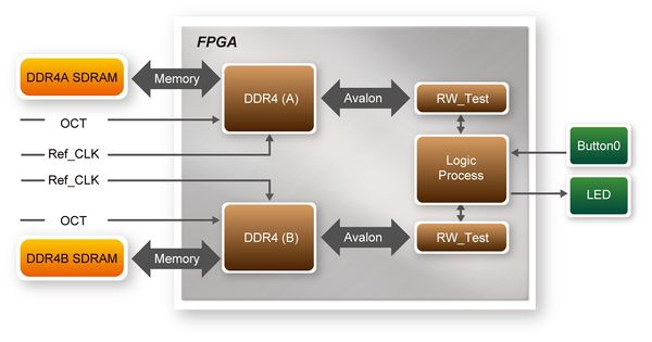
| - | Figure | + | Figure 1-1 shows the function block diagram of this demonstration. There are two DDR4 SDRAM controllers. The controller uses 266.667 MHz as a reference clock. It generates one 1066MHz clock as memory clock from the FPGA to the memory and the controller itself runs at quarter-rate in the FPGA i.e. 266.667 MHz. |
| + | |||
| + | [[File:De10 advanced revc ddr4 rtl block diagram.jpg|600px]] | ||
| - | Figure | + | ::::'''Figure 1-1 Block diagram of DDR4 x2 demonstration''' |
=Design Tools= | =Design Tools= | ||
| - | + | *Quartus Prime 18.0.0 Standard Edition | |
| - | + | *Demonstration Source Code: | |
| - | + | **Project Directory: Demonstration\RTL_DDR4 | |
| - | + | **Bit Stream: RTL_DDR4.sof | |
| - | + | ||
| + | =Demonstration Batch File= | ||
Demo Batch File Folder: RTL_DDR4 \demo_batch | Demo Batch File Folder: RTL_DDR4 \demo_batch | ||
The demo batch file includes following files: | The demo batch file includes following files: | ||
| - | + | *Batch File: test.bat | |
| - | + | *FPGA Configuration File: RTL_DDR4.sof | |
=Demonstration Setup= | =Demonstration Setup= | ||
| + | #Make sure Quartus Prime is installed on the host PC. | ||
| + | #Connect DE10-Advanced board to the host PC via USB cable. Install the USB-Blaster II driver if necessary. | ||
| + | #Power on the DE10-Advanced. | ||
| + | #Execute the demo batch file “test.bat” under the batch file folder \ RTL_DDR4\demo_batch. | ||
| + | #Press KEY0 on DE10-Advanced to start the verification process. When KEY0 is released, LED0, LED1 should start blinking. After approximately 2 seconds, LED1 and LED2 should stop blinking and stay on to indicate the DDR4 (A) and DDR4 (B) have passed the test, respectively. Table 6-2 lists the LED indicators. | ||
| + | #If LED0 or LED1 does not start blinking upon releasing KEY0, it indicates local_cal_success of the corresponding DDR4 fails. | ||
| + | #If LED0 or LED1 fail to remain on after 2 seconds, the corresponding DDR4 test has failed. | ||
| + | #Press KEY0 again to regenerate the test control signals for a repeat test. | ||
| + | |||
| + | |||
| + | :'''Table 1-1 LED Indicators''' | ||
| + | :{| class="wikitable" | ||
| + | |- | ||
| + | !NAME !!Description | ||
| + | |- | ||
| + | |LED0 ||DDR4 (A) test result | ||
| + | |- | ||
| + | |LED1 ||DDR4 (B) test result | ||
| + | |} | ||
| - | + | '''[[DE10-Advance_Demonstration_Manual_revC#Chapter 2 Examples For FPGA|Back]]''' | |
| - | + | ||
| - | + | ||
| - | + | ||
| - | + | ||
| - | + | ||
| - | + | ||
| - | + | ||
| - | + | ||
| - | + | ||
| - | + | ||
| - | + | ||
Latest revision as of 16:27, 24 August 2018
This demonstration performs a memory test function on the one DDR4 SO-DIMM (DDR4A) and one DDR4 Component (DDR4B) on the DE10-Advanced. The memory size of DDR4 SO-DIMM is 4GB and DDR4 Component is 1GB.
Contents |
Function Block Diagram
Figure 1-1 shows the function block diagram of this demonstration. There are two DDR4 SDRAM controllers. The controller uses 266.667 MHz as a reference clock. It generates one 1066MHz clock as memory clock from the FPGA to the memory and the controller itself runs at quarter-rate in the FPGA i.e. 266.667 MHz.
- Figure 1-1 Block diagram of DDR4 x2 demonstration
Design Tools
- Quartus Prime 18.0.0 Standard Edition
- Demonstration Source Code:
- Project Directory: Demonstration\RTL_DDR4
- Bit Stream: RTL_DDR4.sof
Demonstration Batch File
Demo Batch File Folder: RTL_DDR4 \demo_batch
The demo batch file includes following files:
- Batch File: test.bat
- FPGA Configuration File: RTL_DDR4.sof
Demonstration Setup
- Make sure Quartus Prime is installed on the host PC.
- Connect DE10-Advanced board to the host PC via USB cable. Install the USB-Blaster II driver if necessary.
- Power on the DE10-Advanced.
- Execute the demo batch file “test.bat” under the batch file folder \ RTL_DDR4\demo_batch.
- Press KEY0 on DE10-Advanced to start the verification process. When KEY0 is released, LED0, LED1 should start blinking. After approximately 2 seconds, LED1 and LED2 should stop blinking and stay on to indicate the DDR4 (A) and DDR4 (B) have passed the test, respectively. Table 6-2 lists the LED indicators.
- If LED0 or LED1 does not start blinking upon releasing KEY0, it indicates local_cal_success of the corresponding DDR4 fails.
- If LED0 or LED1 fail to remain on after 2 seconds, the corresponding DDR4 test has failed.
- Press KEY0 again to regenerate the test control signals for a repeat test.
- Table 1-1 LED Indicators
NAME Description LED0 DDR4 (A) test result LED1 DDR4 (B) test result
