DE10 Advance revC demo: Users LED and KEY
From Terasic Wiki
| Line 1: | Line 1: | ||
This demonstration shows how to control the users LED and KEY by accessing the register of GPIO controller through the memory-mapped device driver. The memory-mapped device driver allows developer to access the system physical memory. | This demonstration shows how to control the users LED and KEY by accessing the register of GPIO controller through the memory-mapped device driver. The memory-mapped device driver allows developer to access the system physical memory. | ||
| - | + | *'''Function Block Diagram''' | |
| - | Figure 3-1 shows the function block diagram of this demonstration. The users LED and KEY are connected to the GPIO1 controller in HPS. The behavior of GPIO controller is controlled by the register in GPIO controller. The registers can be accessed by application software through the memory-mapped device driver, which is built into Intel SoC Linux. <br/> | + | Figure 3-1 shows the function block diagram of this demonstration. The users LED and KEY are connected to the '''GPIO1''' controller in HPS. The behavior of GPIO controller is controlled by the register in GPIO controller. The registers can be accessed by application software through the memory-mapped device driver, which is built into Intel SoC Linux. <br/> |
:::[[File:Block diagram of GPIO demonstration.jpg|600px]] | :::[[File:Block diagram of GPIO demonstration.jpg|600px]] | ||
::::::::::Figure 3-1 Block diagram of GPIO demonstration | ::::::::::Figure 3-1 Block diagram of GPIO demonstration | ||
| - | + | *'''Block Diagram of GPIO Interface''' | |
The HPS provides three general-purpose I/O (GPIO) interface modules. Figure 3-2 shows the block diagram of GPIO Interface. GPIO[28..0] is controlled by the GPIO0 controller and GPIO[57..29] is controlled by the GPIO1 controller. GPIO[70..58] and input-only GPI[13..0] are controlled by the GPIO2 controller. | The HPS provides three general-purpose I/O (GPIO) interface modules. Figure 3-2 shows the block diagram of GPIO Interface. GPIO[28..0] is controlled by the GPIO0 controller and GPIO[57..29] is controlled by the GPIO1 controller. GPIO[70..58] and input-only GPI[13..0] are controlled by the GPIO2 controller. | ||
:::[[File:Block diagram of GPIO Interface.jpg|600px]] | :::[[File:Block diagram of GPIO Interface.jpg|600px]] | ||
:::::::::Figure 3-2 Block diagram of GPIO Interface | :::::::::Figure 3-2 Block diagram of GPIO Interface | ||
| - | + | *'''GPIO Register Block''' | |
The behavior of I/O pin is controlled by the registers in the register block. There are three 32-bit registers in the GPIO controller used in this demonstration. The registers are: | The behavior of I/O pin is controlled by the registers in the register block. There are three 32-bit registers in the GPIO controller used in this demonstration. The registers are: | ||
| - | *gpio_swporta_dr: write output data to output I/O pin | + | *'''gpio_swporta_dr''': write output data to output I/O pin |
| - | *gpio_swporta_ddr: configure the direction of I/O pin | + | *'''gpio_swporta_ddr''': configure the direction of I/O pin |
| - | *gpio_ext_porta: read input data of I/O input pin | + | *'''gpio_ext_porta''': read input data of I/O input pin |
| - | The gpio_swporta_ddr configures the LED pin as output pin and drives it high or low by writing data to the gpio_swporta_dr register. The first bit (least significant bit) of gpio_swporta_ddr controls the direction of first IO pin in the associated GPIO controller and the second bit controls the direction of second IO pin in the associated GPIO controller and so on. The value "1" in the register bit indicates the I/O direction is output, and the value "0" in the register bit indicates the I/O direction is input. <br/><br/> | + | The '''gpio_swporta_ddr''' configures the LED pin as output pin and drives it high or low by writing data to the '''gpio_swporta_dr''' register. The first bit (least significant bit) of '''gpio_swporta_ddr''' controls the direction of first IO pin in the associated GPIO controller and the second bit controls the direction of second IO pin in the associated GPIO controller and so on. The value "1" in the register bit indicates the I/O direction is output, and the value "0" in the register bit indicates the I/O direction is input. <br/><br/> |
| - | The first bit of gpio_swporta_dr register controls the output value of first I/O pin in the associated GPIO controller, and the second bit controls the output value of second I/O pin in the associated GPIO controller and so on. The value "1" in the register bit indicates the output value is high, and the value "0" indicates the output value is low. <br/><br/> | + | The first bit of '''gpio_swporta_dr''' register controls the output value of first I/O pin in the associated GPIO controller, and the second bit controls the output value of second I/O pin in the associated GPIO controller and so on. The value "1" in the register bit indicates the output value is high, and the value "0" indicates the output value is low. <br/><br/> |
| - | The status of KEY can be queried by reading the value of gpio_ext_porta register. The first bit represents the input status of first IO pin in the associated GPIO controller, and the second bit represents the input status of second IO pin in the associated GPIO controller and so on. The value "1" in the register bit indicates the input state is high, and the value "0" indicates the input state is low. | + | The status of KEY can be queried by reading the value of '''gpio_ext_porta''' register. The first bit represents the input status of first IO pin in the associated GPIO controller, and the second bit represents the input status of second IO pin in the associated GPIO controller and so on. The value "1" in the register bit indicates the input state is high, and the value "0" indicates the input state is low. |
| - | + | *'''GPIO Register Address Mapping''' | |
The registers of HPS peripherals are mapped to HPS base address space 0xFC000000 with 64MB size. The registers of the GPIO1 controller are mapped to the base address 0xFFC02A00 with 256B size, and the registers of the GPIO2 controller are mapped to the base address 0xFFC02B00 with 256B size, as shown in Figure 3-3. <br/> | The registers of HPS peripherals are mapped to HPS base address space 0xFC000000 with 64MB size. The registers of the GPIO1 controller are mapped to the base address 0xFFC02A00 with 256B size, and the registers of the GPIO2 controller are mapped to the base address 0xFFC02B00 with 256B size, as shown in Figure 3-3. <br/> | ||
:::[[File:GPIO address map.jpg|600px]] | :::[[File:GPIO address map.jpg|600px]] | ||
::::::::::Figure 3-3 GPIO address map | ::::::::::Figure 3-3 GPIO address map | ||
| - | + | *'''Software API''' | |
Developers can use the following software API to access the register of GPIO controller. <br> | Developers can use the following software API to access the register of GPIO controller. <br> | ||
| - | *open: open memory mapped device driver | + | *'''open''': open memory mapped device driver |
| - | *mmap: map physical memory to user space | + | *'''mmap''': map physical memory to user space |
| - | *alt_read_word: read a value from a specified register | + | *'''alt_read_word''': read a value from a specified register |
| - | *alt_write_word: write a value into a specified register | + | *'''alt_write_word''': write a value into a specified register |
| - | *munmap: clean up memory mapping | + | *'''munmap''': clean up memory mapping |
| - | *close: close device driver | + | *'''close''': close device driver |
Developers can also use the following MACRO to access the register. | Developers can also use the following MACRO to access the register. | ||
| - | *alt_setbits_word: set specified bit value to one for a specified register | + | *'''alt_setbits_word''': set specified bit value to one for a specified register |
| - | *alt_clrbits_word: set specified bit value to zero for a specified register | + | *'''alt_clrbits_word''': set specified bit value to zero for a specified register |
The program must include the following header files to use the above API to access the registers of GPIO controller. | The program must include the following header files to use the above API to access the registers of GPIO controller. | ||
::include <stdio.h> | ::include <stdio.h> | ||
| Line 47: | Line 47: | ||
::include "socal/alt_gpio.h" | ::include "socal/alt_gpio.h" | ||
| - | + | *'''LED and KEY Control''' | |
Figure 3-4 shows the HPS users LED and KEY pin assignment for the DE10_Advanced board. The LED is connected to GPIO1_IO1 and the KEY is connected to GPIO1_IO4. | Figure 3-4 shows the HPS users LED and KEY pin assignment for the DE10_Advanced board. The LED is connected to GPIO1_IO1 and the KEY is connected to GPIO1_IO4. | ||
:::[[File:Pin assignment of LED and KEY.jpg|600px]] | :::[[File:Pin assignment of LED and KEY.jpg|600px]] | ||
::::::::Figure 3-4 Pin assignment of LED and KEY | ::::::::Figure 3-4 Pin assignment of LED and KEY | ||
| - | Figure 3-5 shows the gpio_swporta_ddr register of the GPIO1 controller. The bit-0 controls the pin direction of GPIO1_IO0. The bit-1 controls the pin direction of GPIO1_IO1, which connects to HPS_LED, the bit-4 controls the pin direction of GPIO1_IO4, which connects to HPS_KEY and so on. The pin direction of HPS_LED and HPS_KEY are controlled by the bit-1 and bit-4 in the gpio_swporta_ddr register of the GPIO1 controller, respectively. Similarly, the output status of HPS_LED is controlled by the bit-1 in the gpio_swporta_dr register of the GPIO1 controller. The status of KEY can be queried by reading the value of the bit-4 in the gpio_ext_porta register of the GPIO1 controller. | + | Figure 3-5 shows the '''gpio_swporta_ddr''' register of the GPIO1 controller. The bit-0 controls the pin direction of GPIO1_IO0. The bit-1 controls the pin direction of GPIO1_IO1, which connects to HPS_LED, the bit-4 controls the pin direction of GPIO1_IO4, which connects to HPS_KEY and so on. The pin direction of HPS_LED and HPS_KEY are controlled by the bit-1 and bit-4 in the '''gpio_swporta_ddr''' register of the GPIO1 controller, respectively. Similarly, the output status of HPS_LED is controlled by the bit-1 in the '''gpio_swporta_dr''' register of the GPIO1 controller. The status of KEY can be queried by reading the value of the bit-4 in the '''gpio_ext_porta''' register of the GPIO1 controller. |
:::[[File:Gpio swporta ddr register in the GPIO1 controller.jpg|600px]] | :::[[File:Gpio swporta ddr register in the GPIO1 controller.jpg|600px]] | ||
::::::::Figure 3-5 Gpio swporta ddr register in the GPIO1 controller | ::::::::Figure 3-5 Gpio swporta ddr register in the GPIO1 controller | ||
| Line 63: | Line 63: | ||
The following statement is used to turn on the LED. | The following statement is used to turn on the LED. | ||
::alt_clrbits_word( ( virtual_base + ALT_GPIO_SWPORTA_DR_OFST ), BIT_LED ); | ::alt_clrbits_word( ( virtual_base + ALT_GPIO_SWPORTA_DR_OFST ), BIT_LED ); | ||
| - | The following statement is used to read the content of gpio_ext_porta register. The bit mask is used to check the status of the key. | + | The following statement is used to read the content of '''gpio_ext_porta''' register. The bit mask is used to check the status of the key. |
::alt_read_word( virtual_base + ALT_GPIO_EXT_PORTA_OFST ); | ::alt_read_word( virtual_base + ALT_GPIO_EXT_PORTA_OFST ); | ||
| - | + | *'''Demonstration Source Code''' | |
| - | *Build tool: SoC EDS V18.0 | + | :*'''Build tool''': SoC EDS V18.0 |
| - | *Project directory: \Demonstration\SoC\hps_gpio | + | :*'''Project directory''': \Demonstration\SoC\hps_gpio |
| - | *Binary file: hps_gpio | + | :*'''Binary file''': hps_gpio |
| - | *Build command: make ('make clean' to remove all temporal files) | + | :*'''Build command''': make ('make clean' to remove all temporal files) |
| - | *Execute command: ./hps_gpio | + | :*'''Execute command''': ./hps_gpio |
| - | + | *'''Demonstration Setup''' | |
*Connect a USB cable to the USB-to-UART connector (J27) on the DE10_Advanced board and the host PC. | *Connect a USB cable to the USB-to-UART connector (J27) on the DE10_Advanced board and the host PC. | ||
| - | *Copy the executable file "hps_gpio" into the microSD card under the "/home/root" folder in Linux. | + | *Copy the executable file "'''hps_gpio'''" into the microSD card under the '''"/home/root'''" folder in Linux. |
*Insert the booting micro SD card into the DE10_Advanced board. | *Insert the booting micro SD card into the DE10_Advanced board. | ||
*Power on the DE10_Advanced board. | *Power on the DE10_Advanced board. | ||
| - | *Launch Putty and establish connection to the UART port of Putty. Type "root" to login into Linux. | + | *Launch Putty and establish connection to the UART port of Putty. Type "'''root'''" to login into Linux. |
| - | *Type "./hps_gpio " in the UART terminal of Putty to start the program. | + | *Type '''"./hps_gpio''' " in the UART terminal of Putty to start the program. |
:[[File:Figure 3-5.jpg|500px]] | :[[File:Figure 3-5.jpg|500px]] | ||
*HPS_LED will flash twice and users can control the user LED with push-button. | *HPS_LED will flash twice and users can control the user LED with push-button. | ||
Revision as of 17:21, 27 August 2018
This demonstration shows how to control the users LED and KEY by accessing the register of GPIO controller through the memory-mapped device driver. The memory-mapped device driver allows developer to access the system physical memory.
- Function Block Diagram
Figure 3-1 shows the function block diagram of this demonstration. The users LED and KEY are connected to the GPIO1 controller in HPS. The behavior of GPIO controller is controlled by the register in GPIO controller. The registers can be accessed by application software through the memory-mapped device driver, which is built into Intel SoC Linux.
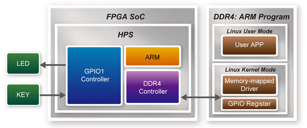
- Figure 3-1 Block diagram of GPIO demonstration

- Block Diagram of GPIO Interface
The HPS provides three general-purpose I/O (GPIO) interface modules. Figure 3-2 shows the block diagram of GPIO Interface. GPIO[28..0] is controlled by the GPIO0 controller and GPIO[57..29] is controlled by the GPIO1 controller. GPIO[70..58] and input-only GPI[13..0] are controlled by the GPIO2 controller.
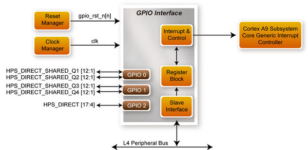
- Figure 3-2 Block diagram of GPIO Interface

- GPIO Register Block
The behavior of I/O pin is controlled by the registers in the register block. There are three 32-bit registers in the GPIO controller used in this demonstration. The registers are:
- gpio_swporta_dr: write output data to output I/O pin
- gpio_swporta_ddr: configure the direction of I/O pin
- gpio_ext_porta: read input data of I/O input pin
The gpio_swporta_ddr configures the LED pin as output pin and drives it high or low by writing data to the gpio_swporta_dr register. The first bit (least significant bit) of gpio_swporta_ddr controls the direction of first IO pin in the associated GPIO controller and the second bit controls the direction of second IO pin in the associated GPIO controller and so on. The value "1" in the register bit indicates the I/O direction is output, and the value "0" in the register bit indicates the I/O direction is input.
The first bit of gpio_swporta_dr register controls the output value of first I/O pin in the associated GPIO controller, and the second bit controls the output value of second I/O pin in the associated GPIO controller and so on. The value "1" in the register bit indicates the output value is high, and the value "0" indicates the output value is low.
The status of KEY can be queried by reading the value of gpio_ext_porta register. The first bit represents the input status of first IO pin in the associated GPIO controller, and the second bit represents the input status of second IO pin in the associated GPIO controller and so on. The value "1" in the register bit indicates the input state is high, and the value "0" indicates the input state is low.
- GPIO Register Address Mapping
The registers of HPS peripherals are mapped to HPS base address space 0xFC000000 with 64MB size. The registers of the GPIO1 controller are mapped to the base address 0xFFC02A00 with 256B size, and the registers of the GPIO2 controller are mapped to the base address 0xFFC02B00 with 256B size, as shown in Figure 3-3.
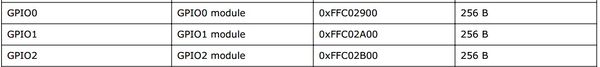
- Figure 3-3 GPIO address map

- Software API
Developers can use the following software API to access the register of GPIO controller.
- open: open memory mapped device driver
- mmap: map physical memory to user space
- alt_read_word: read a value from a specified register
- alt_write_word: write a value into a specified register
- munmap: clean up memory mapping
- close: close device driver
Developers can also use the following MACRO to access the register.
- alt_setbits_word: set specified bit value to one for a specified register
- alt_clrbits_word: set specified bit value to zero for a specified register
The program must include the following header files to use the above API to access the registers of GPIO controller.
- include <stdio.h>
- include <unistd.h>
- include <fcntl.h>
- include <sys/mman.h>
- include "hwlib.h"
- include "socal/socal.h"
- include "socal/hps.h"
- include "socal/alt_gpio.h"
- LED and KEY Control
Figure 3-4 shows the HPS users LED and KEY pin assignment for the DE10_Advanced board. The LED is connected to GPIO1_IO1 and the KEY is connected to GPIO1_IO4.

- Figure 3-4 Pin assignment of LED and KEY

Figure 3-5 shows the gpio_swporta_ddr register of the GPIO1 controller. The bit-0 controls the pin direction of GPIO1_IO0. The bit-1 controls the pin direction of GPIO1_IO1, which connects to HPS_LED, the bit-4 controls the pin direction of GPIO1_IO4, which connects to HPS_KEY and so on. The pin direction of HPS_LED and HPS_KEY are controlled by the bit-1 and bit-4 in the gpio_swporta_ddr register of the GPIO1 controller, respectively. Similarly, the output status of HPS_LED is controlled by the bit-1 in the gpio_swporta_dr register of the GPIO1 controller. The status of KEY can be queried by reading the value of the bit-4 in the gpio_ext_porta register of the GPIO1 controller.
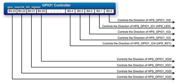
- Figure 3-5 Gpio swporta ddr register in the GPIO1 controller

The following mask is defined in the demo code to control LED and KEY direction and LED’s output value.
- define USER_IO_DIR (0x00000002)
- define BIT_LED (0x00000002)
- define BUTTON_MASK (0x00000010)
The following statement is used to configure the LED associated pins as output pins.
- alt_setbits_word( ( virtual_base + ALT_GPIO_SWPORTA_DDR_OFST ), USER_IO_DIR );
The following statement is used to turn on the LED.
- alt_clrbits_word( ( virtual_base + ALT_GPIO_SWPORTA_DR_OFST ), BIT_LED );
The following statement is used to read the content of gpio_ext_porta register. The bit mask is used to check the status of the key.
- alt_read_word( virtual_base + ALT_GPIO_EXT_PORTA_OFST );
- Demonstration Source Code
- Build tool: SoC EDS V18.0
- Project directory: \Demonstration\SoC\hps_gpio
- Binary file: hps_gpio
- Build command: make ('make clean' to remove all temporal files)
- Execute command: ./hps_gpio
- Demonstration Setup
- Connect a USB cable to the USB-to-UART connector (J27) on the DE10_Advanced board and the host PC.
- Copy the executable file "hps_gpio" into the microSD card under the "/home/root" folder in Linux.
- Insert the booting micro SD card into the DE10_Advanced board.
- Power on the DE10_Advanced board.
- Launch Putty and establish connection to the UART port of Putty. Type "root" to login into Linux.
- Type "./hps_gpio " in the UART terminal of Putty to start the program.

- HPS_LED will flash twice and users can control the user LED with push-button.
- Press HPS_KEY to light on and off the HPS_LED.
- Press "CTRL + C" to terminate the application.