Terasic TR4 FPGA Development Kit
FPGA Devices
Stratix IV GX EP4SGX230
- 228,000 logic elements (LEs)
- 17,133 total memory Kbits
- 1,288 18x18-bit multipliers blocks
- 2 PCI Express hard IP blocks
- 744 user I/Os
- 8 phase locked loops (PLLs)
Stratix IV GX EP4SGX530
- 531,200 logic elements (LEs)
- 27,376 total memory Kbits
- 1,024 18x18-bit multipliers blocks
- 4 PCI Express hard IP Blocks
- 744 user I/Os
- 8 phase locked loops (PLLs)
FPGA Configuration
- MAXII CPLD EPM2210 System Controller and Fast Passive Parallel (FPP) configuration
- On-board USB Blaster for use with the Quartus II Programmer
- Programmable PLL timing chip configured via MAX II CPLD
- Supports JTAG mode
Memory Devices
- 64MB Flash with a 16-bit data bus
- 2MB SSRAM (512K x 32)
DDR3 SO-DIMM Socket
- Up to 8GB capacity
- Maximum memory clock rate at 533MHz
- Theoretical bandwidth up to 68Gbps
Buttons, Switches and LEDs
- 4 user-controllable LEDs
- 4 buttons for user-defined inputs
- 4 slide switches for user-defined inputs
On-Board Clocks
SMA Connectors
- SMA connector pair for differential clock inputs
- SMA connector pair for differential clock outputs
- SMA connector for clock output
- SMA connector for external clock input
Two PCI Express x4 Connectors
- Support connection speed of Gen1 at 2.5Gbps/lane to Gen2 at 5.0Gbps/lane
- High-speed transceiver channels up to 6.5 Gbps
- Support downstream mode
Six 172-pins High Speed Mezzanine Card (HSMC)
- 6 HSMC connectors
- Configurable I/O standards - 1.5V, 1.8V, 2.5V, 3.0V
- Total of 16 high-speed transceivers up to 6.5 Gbps
- Among HSMC Port A to D, there are 55 true LVDS TX channels to 1.6Gbps and 17 emulated LVDS TX channels up to 1.1Gbps
Two 40-pin Expansion Headers
- 72 FPGA I/O pins; 4 power and ground lines
- Configurable I/O standards - 1.5V, 1.8V, 2.5V, 3.0V
- Shares pins with HSMC Port
Power
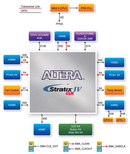
Block Diagram


