Altera Stratix V GX FPGA Development Kit
Featured device:
- Stratix V GX FPGA: 5SGXEA7K2F40C2N
Configuration, status, and setup elements
- JTAG
- On-board USB-BlasterTM II cable
- Fast passive parallel (FPP) configuration via MAX®
V device and flash memory
- One reset config push button
- One CPU reset push button
- Two configuration push buttons
Clocks
- 50-MHz, 125-MHz, 100-MHz, and 148.5-MHz programmable oscillators
- SMA input (LVPECL)
General user input and output
- 10/100/1000Mbps Ethernet PHY (SGMII) with RJ-45 (copper) connector
- 16x2 character LCD
- One 8-position dual in-line package (DIP) switch
- Sixteen user LEDs
- Three user push buttons
Memory devices
- DDR3 SDRAM (1,152 MB, x72-bit wide)
- QDR II+ SRAM (4.5 MB, 2-Mb x18-bit wide)
- Footprint compatible to QDR II 4-Mb x18-bit wide
- RLDRAM II (72-Mbyte CIO RLDRAM II with an 18-bit data bus)
Component and interfaces
- PCIe x8 edge connector
- Two HSMC connectors
- SMB for serial digital interface (SDI) input and output
- QSFP optical cage
- 10/100/1000Mbps Ethernet PHY (SGMII) with RJ-45 (copper) connector
Power
- Laptop DC input
- PCIe edge connector
- Nios®
II processor web server and remote system update
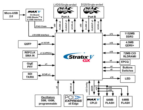
Stratix V GX FPGA Development Board Block Diagram