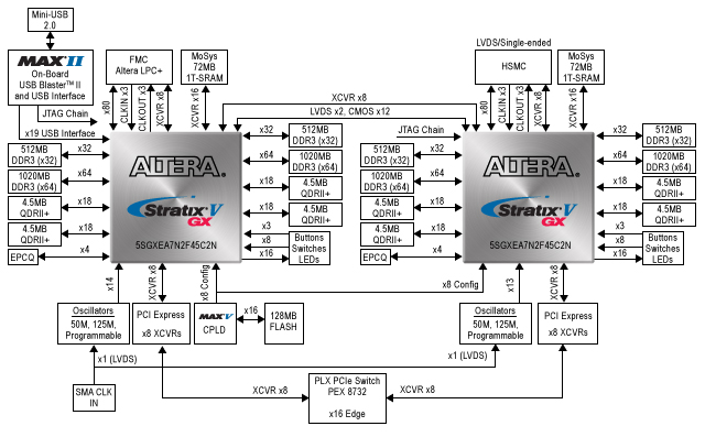
Altera Stratix V Advanced Systems Development Kit
Featured devices
- 5SGXEA7N2F45C2N = FPGA 1
- 5SGXEA7N2F45C2N = FPGA 2
- 5M2210ZF256C4N system controller
- EPM570F100C5N on-board USB-BlasterTM
II cable
External memory interfaces
- FPGA 1
- 3072 MB 2x64+2x32 DDR3 SDRAM
- 9 MB 2x18 QDRII+ SDRAM
- 72 MB 4x72 MoSYS SRAM (10x10G XCVR)
- 32 MB serial flash
- FPGA 2
- 3072 MB 2x64+2x32 DDR3 SDRAM
- 9 MB 2x18 QDRII+ SDRAM
- 72 MB 4x72 MoSYS SRAM (10x10G XCVR)
- 32 MB serial flash
- CPLD
- 1 GB parallel flash for PFL
Clocks
- 50 MHz, 100 MHz, and 125 MHz programmable oscillators
- SMA input (LVDS)
General user input and output
- Each FPGA has 1 8-position dual in-line package (DIP) switch
- Each FPGA has 16 user LEDs
- Each FPGA has 3 user push buttons
Communication interfaces
- PCIe x16 edge connector to PLX PE8747 Gen3 Switch
- One PCIe Gen3 x8 to each FPGA
- 1 FMC connector (FPGA 1)
- 1 HSMC port (FPGA 2)
- USB 2.0 on-board USB-Blaster II cable
Power
- Laptop DC input
- PCIe edge connector
Altera Stratix V Advanced Systems Development Board Block Diagram


