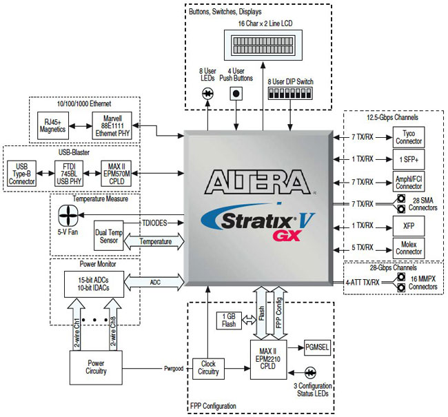
Altera Transceiver Signal Integrity Development Kit, Stratix V GT Edition
Featured device
Configuration status and set-up elements
- JTAG
- On-board USB-BlasterTM
- Fast passive parallel (FPP) configuration via MAX®
II device and flash memory
- Two configuration file storage
- Temperature measurement circuitry (die and ambient temperature)
Clocks
- 50 MHz, 125 MHz, programmable oscillators (preset values: 624 MHz, 644.5 MHz, 706.25 MHz, and 875 MHz)
- SMA connectors for supplying an external differential clock to transceiver reference clock
- SMA connectors for supplying an external differential clock to the FPGA fabric
- SMA connectors to output a differential clock from the FPGA's phase-locked loop (PLL) output pin
General user input/output
- 10-/100-/1000-Mbps Ethernet PHY (RGMII) with RJ-45 (copper) connector
- 16x2 character LCD
- One 8-postion dipswitch
- Eight user LEDs
- Four user pushbuttons
Memory devices
- 128-megabyte (MB) sync flash memory (primarily to store FPGA configurations)
High speed serial interfaces
- Four full-duplex GTB (28.05 Gbps) transceiver channels routed to MMPX connectors
- Seven full-duplex GXB (12.5 Gbps) transceiver channels routed to SMA connectors
- Short trace routed on a micro-strip
- Six strip-line channels from the with all the trace lengths are matched across channels
- 21 full-duplex GXB transceiver channels routed to backplane connector
- Seven channels to Molex®
Impact®
connector
- Seven channels to Amphenol®
XCede®
- Seven channels to footprint of Tyco Strada®
Whisper®
(connector is not populated)
Power
- Laptop DC input
- Voltage margining
Stratix V GX Transceiver Signal Integrity Development Board Block Diagram


