Documents
| Title | Version | Size | Date | Download |
|---|---|---|---|---|
| Data Conversion HSMC reference manual | 1.0.1 | 712(KB) | 2011-07-01 |
CD-ROM
| Title | Version | Size | Date | Download |
|---|---|---|---|---|
| AD/DA Data Conversion Card CD-ROM | 1.0.1 | 2011-07-01 |
Please note that all the source codes are provided "as-is". For further support or modification, please contact Terasic Support and your request will be transferred to Terasic Design Service.
More resources about IP and Dev. Kit are available on Intel User Forums.
Transmission Demo
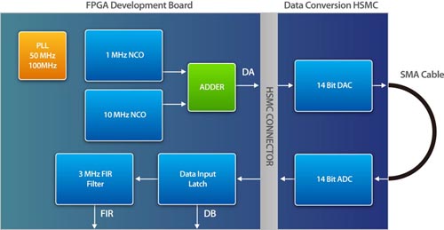
The AD/DA Data Conversion CD includes a reference design which contains two sine waves that are generated by two instances of the Altera numerically controlled oscillator (NCO) MegaCore. One of these oscillators is running at 10 times the frequency of the other, but both of them have the same amplitude with each one covering 13 bits of dynamic range. From these blocks, the two sine waves output are converted from two’s complement binary to unsigned binary format which then are added together. The combined sine wave signal of 14-bits dynamic range is sent to a 14-bit D/A converter. The analog output of a D/A converter is connected via SMA Cable with the analog input of a 14-bit A/D converter. The A/D converter’s digital output is looped back to the FPGA device. The A/D is configured by the dip switches to deliver the data in unsigned format. The converted loopback data is captured by an instance of the SignalTap® II logic analyzer in the design for display and analysis.
The following figure below shows a high-level view of the reference design and how it interacts with the D/A and A/D converters on the AD/DA Data Conversion Card in the following sections.
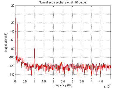
You can use MATLAB software to analyze the data.
The following figure below is generated using SignalTap to capture and analyze data.


