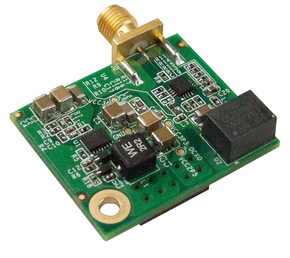
The OTB is a daughter card that provides maximum precision thermostat clock frequency signal outputs to the FPGA motherboard. It provides high-performance clock sources for the FPGA. The clock source that is used by the daughter card is OCXO (Oven-controlled crystal oscillator). The clock outputs use an SMA interface. Users can send clock signals through an SMA input connector on the FPGA motherboard via SMA to SMA cable, such as the DE5-NET. If there is a height limitation on a user’s project design, the user can also send clock signals via the SMA to U.FL Cable or the U.FL cable to SMA adapter to send the clock signals to any motherboards with an SMA connector.
The OTB mainly provides power through the JTAG header. It can be connected to a motherboard with a 2x5 built-in JTAG header.

