Apollo S10 User Manual revA CH1
From Terasic Wiki
This chapter provides an overview of the Apollo S10 Development Board and installation guide.
Contents |
1.1 General Description
待寫
1.2 Board Layout
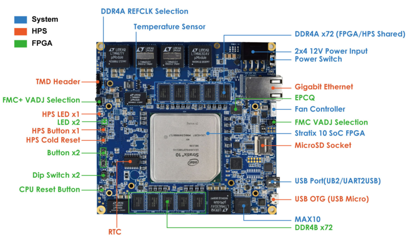
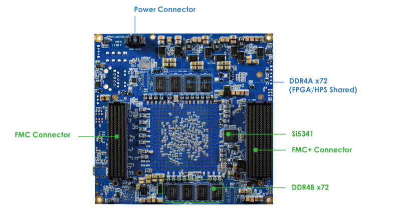
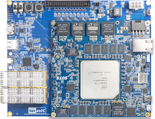
The figures below depict the layout of the board and indicates the location of the connectors and key components.
1.3 Key Features
- FPGA Device
- Intel Stratix ® 10 SoC FPGA : 1SX280HU2F50
- 2,800K logic elements (LEs)
- 229 Mbits embedded memory(M20K)
- 96 transceivers (up to 28.3Gbps)
- 11,520 18-bit x 19-bit multipliers
- 5,760 Variable-precision DSP blocks
- Intel Stratix ® 10 SoC FPGA : 1SX280HU2F50
- FPGA Configuration
- On-Board USB Blaster II for FPGA programming and Debug
- AS Mode configuration from QSPI Flash
- FPGA Fabric
- 1024Mbit QSPI Flash (EPCQL1024 Compliant)
- 2 independent DDR4 banks with ECC.
- Each 16GB Dual Rank DDR4-2666.
- One bank is shared with FPGA and HPS
- DDR4A REFCLK Selection
- FMC (Vita57.1) connector with 10 transceivers
- FMC VADJ 1.8V/1.5V/1.2V Selection
- FMC+(Vita57.4) connector with 24 transceivers
- FMC+ VADJ 1.8V/1.5V/1.2V Selection
- Four 50Mhz Single-ended Clock Source
- One 100Mhz Single-ended Clock Source
- Clock Generator Si5341
- LED x2, Button x2, Dip Switch x2, CPU Reset
- HPS(Hard Processor System) Fabric
- MicroSD Socket
- Gigabit Ethernet with RJ45
- USB OTG with Micro USB Connector
- UART to USB with Mini USB Connector
- RTC
- LED x1, Button x1, Cold Reset Button
- 1x6 TMD Header
- Dashboard System
- Input Power Monitor
- FPGA and Board Temperature Monitor
- Fan Control and Monitor
- Auto Fan Speed
- Auto Shutdown
- Power Source
- 12V from 2x4 PCIe connector
- 12V from Samtec connector (reserved for carrier board)
1.4. Block Diagram
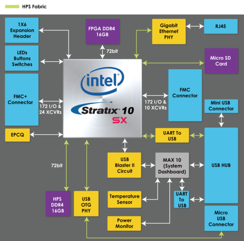
The figure below shows the block diagram of the DE10-Pro SX board. To provide maximum flexibility for the users, all key components are connected to the Stratix ®10 SX FPGA device. Thus, users can configure the FPGA to implement any system design.
1.5 Connectivty
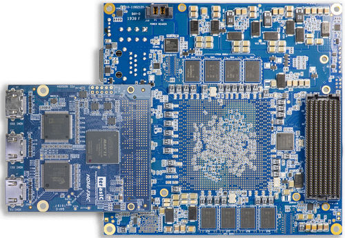
The Apoolo-S10 board provides FMC and FMC + connector as expansion interface. Users can use Apoolo-S10 as stand alone, connect FMC daughter card.
Users can also use Apollo-S10 as an FPGA module board and connect to other base boards to form a system.
