BAL Battery Package 03 Hardware Manual
From Terasic Wiki
Chpater1 Introduction
Terasic's Self-Balancing Robot is a multi-functional robot designed and manufacturered by Terasic robtic exeperts. Built on Terasic's DE10-Nano, a light-weighted SoC platform ideal for embedded solution, and equipped with the state-of-the-art control algorithm, the robot offers developers a perfect starting point to create their own robotic innovations.
This robot can perform posture recognition in real time through the acceleration sensor and the gyroscope, and achieve the balance by controlling the motors to adjust the posture. The Robot can implement attitude algorithm, perform motion control, and execute movements autonomously, such as moving forward, turning right & left, object following and obstacle avoidance.
Self-Balancing Robot equips Bluetooth/Wi-Fi module and IR Receiver, users can remote control robot by smartphone APP and IR remote controller.
There are many peripheral interfaces (Ethernet port, UART port, HDMI-TX port, GPIO connector, USB Blaster II port) on DE10-Nano board for customers development. Besides the hardware, the robot also includes open source examples. Based on the example codes, developers can quickly implement their application designs.
The robot is powered by three sections of lithium battery. If lithium battery starts charging when it is completely unable to supply the robot, it is expected to take up to 2 hours for fully charging.
Chpater2 Key Boards of the Self-Balancing Robot
This chapter briefly introduces the two main control boards DE10-Nano and Motor Driver Board on the Self-Balancing Robot.
2-1 Overview
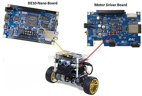
The Self-Balancing Robot control system consist two boards, Terasic DE10-Nano SoC FPGA board and Motor Driver board (See Figure 2 -1).
DE10-Nano board is responsible for the entire Self-Balancing Robot control system, user can use the Nios system or ARM CPU to execute the robot balance algorithm and control other hardware on the robot through SoC FPGA.
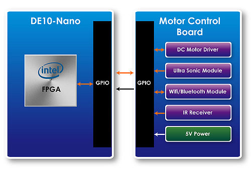
Motor Driver board is responsible for receiving motor control signal from DE10-Nano board, and controlling the motor through the motor driver chip, besides, it receives control signal of Wi-Fi, Bluetooth and IR protocol, then transmits the signal to DE10-Nano for further processing. The motor driver board provides states data to DE10-Nano board via sensors, such as tilt angle of robot body, battery voltage and distance information from ultrasonic module.
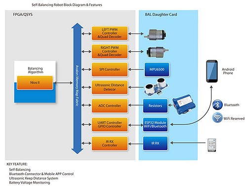
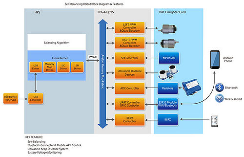
Figure 2-2 shows the block diagram of the robot that uses Nios to control the robot system. Figure 2-3 shows the block diagram of the robot which use ARM CPU to control the robot system.
Chpater3 DE10-Nano Board
This chapter will introduce the main devices of the DE10-Nano on the Self-Balancing Robot.
3-1 Overview
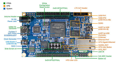
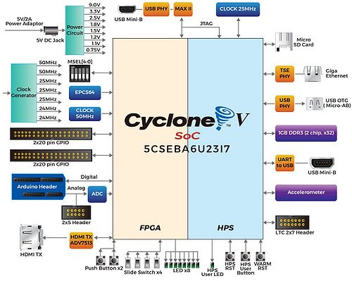
Terasic DE10-Nano board presents a robust hardware design platform built around the Intel Cyclone V SoC FPGA, beside to being used as traditional FPGA, it also combines the dual-core Cortex-A9 processor and related controller. User can run Linux OS on DE10-Nano board, the board provides powerful control and communication ability. Designed with small size and lower power consumption, it is an excellent platform to develop portable applications. Figure 3-4 shows the DE10-Nano board layout, Figure 3-5 shows the system block diagram of DE10-Nano. User can refer to the following link for more detailed information about DE10-Nano board:
http://www.terasic.com.tw/cgi-bin/page/archive.pl?Language=English&CategoryNo=167&No=1046&PartNo=4
Before developing the robot application, users need to get familiar with FPGA develop tools and process, master how to use DE10-Nano board, such as creating Quartus project, using Nios and Qsys tools, mastering advanced skill (i.e. using ARM CPU in the SoC FPGA). Below sections describe th e considerations that needs to be paid attention to when using DE10-Nano on Self-Balancing Robot and some commonly used interfaces on DE10-Nano.
3-2 The DE10-Nano for Self-Balancing Robot
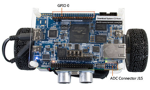
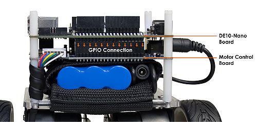
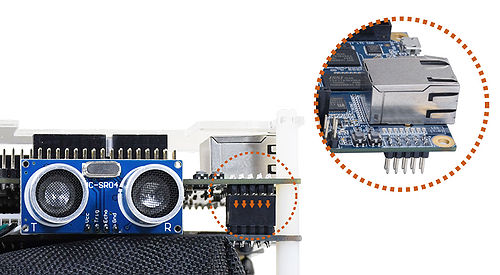
The DE10-Nano board used on the robot has a few differences with the retail version of the DE10-Nano on the Terasic website. As shown in Figure 3 -6, the main difference is that the 2x20-pin GPIO connector (GPIO0) and the 2x 5 ADC(J15) connector are on the bottom of the DE10-Nano board on the robot, i.e. compared to the retail version of DE10-Nano board, the GPIO0 and ADC connectors on the DE10-Nano of the robot are the opposite of 180 degrees, which is convenient to connect to motor driver board, as shown in Figure 3 -7.
3-3 2x20 Pin GPIO Connector
The DE10-Nano board has two 2x 20-pin GPIO connectors, GPIO 1 and GPIO 0. The GPIO 1 connector can be used as an extension function. User can use this connector to connect to other devices or daughter cards of the GPIO interface, such as Terasic D8M (800M pixel camera module). As described in last section, The GPIO 0 connector is used to connect motor driver board and transmit motor control signal and other communication/status signal (see Figure 3 -8). In Addition, the motor driver board provides 5V power to DE10-Nano board through the GPIO 0 connector.
For more interface on the motor driver board, please refer to the chapter 4 for detailed.
3-4 ADC Connector
As described in Section 2.2, the ADC connector is soldered on the DE10-Nano board’s bottom side, it can connect to motor driver board conveniently as shown in Figure 3 -9.
The ADC 2x 5 pin connector is connected to A/D converter(LTC2308), finally connected to FPGA. The A/D converter has a 500ksps, 8-channel interface. The battery voltage information on the Self-Balancing robot will be transmitted to FPGA via ADC Connector and motor driver board sensor circuit. The SoC FPGA system can read the battery voltage information and show the value on smartphone APP.
3-5 LEDs
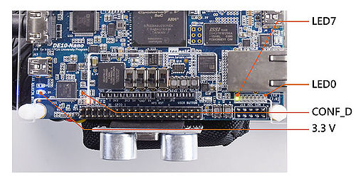
There are some LEDs on the DE10-Nano which can be used for status display or user defined purpose (See Figure 3 -10). Under the factory setting, these LEDs will indicate power status, moving direction, operate mode and so on. Table 3-1 describes the LEDs function.
| LED name | LED status | Description |
| 3.3V power LED | Light On | Power DE10-Nano board with 3.3V from GPIO interface. |
| CONF_D | Light On | DE10-Nano board Configuration done |
| LED7 | Light On | Robot is keeping balance status |
| LED6~5 | 0--Light On
1--Light off
| 00--robot is in default mode (Bluetooth & IR control)
01--robot is in default mode and implements obstacle avoidance function
10--robot implements object following function
|
| LED4 | Light On | Battery power supply voltage is lower than 10V |
| LED3 | Light On | Robot is turning right |
| LED2 | Light On | Robot is turning left |
| LED1 | Light On | Robot is moving backward |
| LED0 | Light On | Robot is moving forward |
3-6 Switches
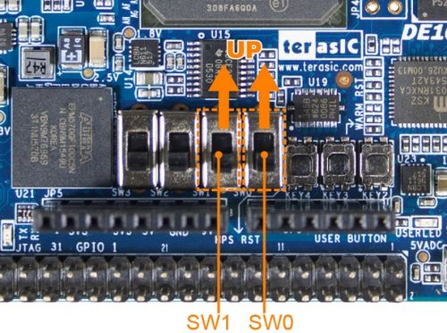
The DE10-Nano board has four slide switches connected to the FPGA, which are allowed to be used as data inputs for robot functions. In the factory setting, these switches are set to switch functions, such as enabling ultrasonic object following and obstacle avoidance, switching to Bluetooth or IR remote control mode. Figure 3-11 shows the SW0 and SW1 on DE10-Nano board, Table 3-2 describes the corresponding modes and functions when SW0 and SW1 are set to different positions.
| SW0&SW1 position | Robot mode and function | Description |
| 00 | Default mode (Bluetooth &IR mode) | The robot can be controlled by smartphone APP and IR remote control |
| 10 | Default mode & Obstacle Avoidance | The robot can be controlled by smartphone APP and IR remote control, it implements the obstacle avoidance function |
| 01 | Object following and obstacle avoidance | The robot implements the object following and obstacle avoidance |
| 11 | Debug mode | Only support ARM version robot, the control program will stop running, user need to reboot the robot or run the program again to control the robot. Normally it is use to debug the robot. |
3-7 USB Blaster II Connector
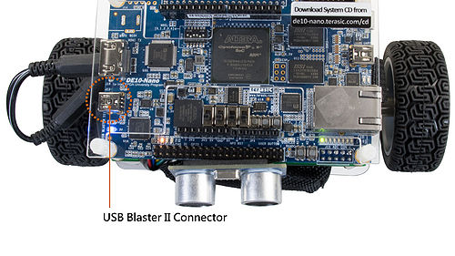
User can configure DE10-Nano SoC FPGA via USB Blaster II connector, use the Singaltab tool (In the Quartus software) to debug, and program the EPCS128 device through JTAG chain. Figure 3-12 shows the USB Blaster II connector. Please refer to Getting_Started_Guide.pdf in the DE10-Nano system CD on how to use the USB Blaster II connector.
3-8 EPCS64 Device
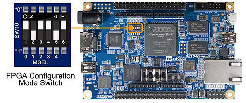
The EPCS64 device is used to configure FPGA automatically when the DE10-Nano board is powered on. As shown in Figure 3 -13, please note the MSEL should be set to AS mode (MSEL[4:0] = "10010") if FPGA is configured from EPCS64, user can use this MSEL setting to control the self-balancing robot via Nios system.
3-9 Micro SD Card
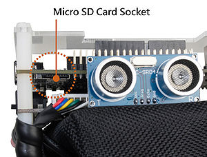
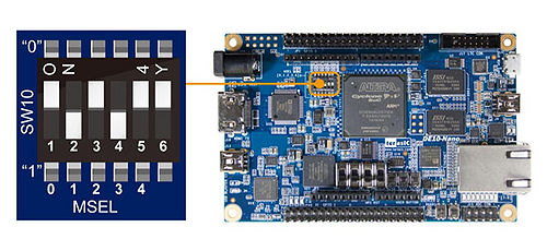
The board supports one Micro SD card socket on HPS side, it’s shown in Figure 3 -14. User can insert the Micro SD card with the pre-built Linux image into the socket and set the MSEL switch to FPP x 32 mode: MSEL [4:0] = "01010", as shown in Figure 3 -15. DE10-Nano board can boot up from the SD card to run Linux OS. User can use this MSEL setting to control the self-balancing robot via ARM system.
3-10 UART to USB
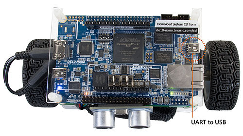
When running Linux OS on the DE10-Nano board, user can connect UART port with PC via Mini-B USB cable and debug. User can refer to Getting_Started_Guide.pdf in the DE10-Nano System CD on how to use the UART port.
3-11 Power Jack on DE10-Nano
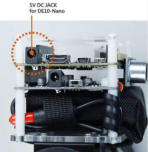
The DE10-Nano board has a 5V power jack used as power input, as shown in Figure 3 -17. The board can be powered through a DC 5V@2A power adapter when user wants to use the DE10-Nano board separately.
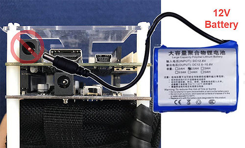
Caution! In the Self-Balancing robot's power system, the DE10-Nano's power supply is provided by the motor driver board via GPIO 0. When using the robot, please do not connect any 5V power supply to this Power JACK. Also, do not use a 12V lithium battery to connect this power jack (See Figure 3 -18).
3-12 Other Interfaces on DE10-Nano Board
Regarding how to use other interfaces on DE10-Nano board, such as HDMI TX, Ethernet and USB OTG, please refer to DE10-Nano_User_manual.pdf and datasheets in the DE10-Nano system CD.
Chpater4 Motor Driver Board
This chapter describes the functions and devices on motor driver board. The main function of this board is receiving motor control signal from FPGA, control the motor through motor control circuit. Besides, the board has communication components, such as Bluetooth and Wi-Fi module, IR remote control, ultrasonic module. The board has analog sensors which can provide motion tracking and battery voltage information.
4-1 Board Layout
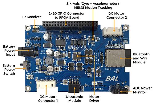
Figure 4-19 shows the layout of the motor driver board.
4-2 Block Diagram
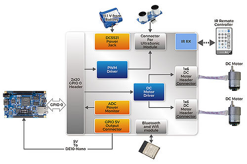
Figure 4-20 shows the block diagram of motor driver board.
4-3 12V Power Jack and Power Switch
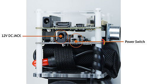
The robot system’s power input connector is located on motor driver board, it’s a 12V DC power jack, as shown in Figure 4-21 which is used to connect 12V battery or power adapter. Note that when using the power adapter to power the robot, please make sure the output current of the power adapter can provide over 1.5A, otherwise the robot may not be able to boot up normally. Once a 12V power source is connected to the power jack on the robot, user can switch system power off and on by the power switch, as shown in Figure 4 -21.
4-4 LEDs on Motor Driver Board
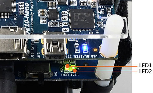
The motor driver board has two LEDs, LED1 and LED2, as shown in Figure 4 -22. They indicate the system 12V power input and DE10-Nano 5V power status, respectively. When LED1 lights on, it indicates the system is powered on by battery or 12V power from power adapter. When LED2 lights on, indicates motor driver board provide 5V power to DE10-Nano board. Table 4-3 describes the functions of LED1 and LED2.
| LED name | Description |
| LED1 | Indicates the power supply status of motor driver board |
| LED2 | Indicates motor driver board provide 5V power to DE10-Nano board |
4-5 GPIO Connector
As described in Section 3.3 GPIO connector on motor driver board is used to connect with DE10-Nano, the corresponding signal information will be described in below sections.
4-6 Bluetooth and Wi-Fi Module
ESP-WROOM-32 is a universal Wi-Fi/Bluetooth/BLE MCU module, it integrates traditional lower power consumption Bluetooth and Wi-Fi features, and has a wide range of uses: the Wi-Fi supports a wide range of communication and also supports connecting to internet directly via router; Bluetooth allows user to connect a cell phone or broadcast BLE Beacon to facilitate signal detection. The module provides several connectors like SPI/SDIO or I2C/UART that are connected to FPGA, as shown in Figure 4 -23, which allows user to communicate with other Wi-Fi or Bluetooth device quickly. The ESP32 module in the self-balancing robot, only UART port (board rate 115200) is used to be connected to the FPGA. Also, only Bluetooth protocol is used for wireless connection. If user want to use the ESP32 with different protocol. User need to re-configure the ESP32 module. Please refer to ESP32 datasheet for details. Table 4-4 describes the pin assignments for connection between ESP32 and FPGA. 8
| ESP32 Signal Name | GPIO Pin No. | DE10-Nano FPGA Pin Assignment | Descriptions | Direction for FPGA | I/O Standard |
| ESP32_EN | 2 | E8 | Chip-enable signal. Active high. | output | 3.3-V |
| ESP32_UART0_TX | 27 | AA19 | UART Transmitter | output | 3.3-V |
| ESP32_UART0_RX | 28 | W11 | UART Receiver | input | 3.3-V |
| ESP32_UART0_RTS | 32 | AA18 | UART Request to Send | output | 3.3-V |
| ESP32_UART0_CTS | 31 | W14 | UART Clear to Send | input | 3.3-V |
| ESP32_CMD0 | 33 | Y18 | GPIO (Reserved) *1 | input | 3.3-V |
| ESP32_CMD1 | 35 | AB25 | GPIO (Reserved) *1 | input | 3.3-V |
| ESP32_CMD2 | 37 | Y11 | GPIO (Reserved) *1 | input | 3.3-V |
| ESP32_CMD3 | 39 | AA13 | GPIO (Reserved) *1 | input | 3.3-V |
| ESP32_CMD4 | 34 | Y17 | GPIO (Reserved) *1 | input | 3.3-V |
| ESP32_CMD5 | 36 | AB26 | GPIO (Reserved) *1 | input | 3.3-V |
| ESP32_CMD6 | 38 | AA26 | GPIO (Reserved) *1 | input | 3.3-V |
| ESP32_CMD7 | 40 | AA11 | GPIO (Reserved) *1 | input | 3.3-V |
| ESP32_CMD8 | 9 | AF4 | GPIO (Reserved) *1 | input | 3.3-V |
*1:Note, ESP32_CMD[8:0] I/Os are reserved for user to set other protocol. user can modify the setting in ESP-WROOM-32 and specify these I/Os as special connectors.
4-7 Motion Tracking Device
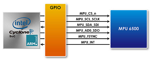
The motor driver board includes one motion tracking device MPU-6500 which plays an important core role. The MPU-6500 contains a 3-axis gyroscope, 3-axis accelerometer and a Digital Motion Processor™ (DMP). The gyroscope can calculate the angular velocity of the 3-axis, the accelerometer can calculate the acceleration of the 3-axis. These two data can be used to determine the tilt angle of the robot as well as the direction and the attitude status of the robot. It is a key parameter to maintain the balance of the robot. The robot can read data stored in MPU-6500 through I2C interface from FPGA. As shown in Figure 4 -24, the I2C address is 0xD2/0xD3. Table 4-5 describes the pin assignments for connection between MPU-6500 and FPGA.
| MPU-6500 Signal Name | GPIO Pin No. | DE10-Nano FPGA Pin Assignment | Descriptions | Direction for FPGA | I/O Standard |
| MPU_CS_n | 17 | AD23 | Chip-enable signal. Active high. | Output | 3.3-V |
| MPU_SCL_SCLK | 19 | D12 | I2C serial clock (SCL); SPI serial clock (SCLK) | Output | 3.3-V |
| MPU_SDA_SDI | 20 | AD20 | I2C serial data (SDA); SPI serial data input (SDI) | Input | 3.3-V |
| MPU_AD0_SDO | 21 | C12 | I2C Slave Address LSB (AD0); SPI serial data output (SDO) | Output | 3.3-V |
| MPU_FSYNC | 22 | AD17 | Frame synchronization digital input. Connect to GND if unused. | Output | 3.3-V |
| MPU_INT | 1 | V12 | Interrupt digital output | Input | 3.3-V |
4-8 Motor Driver
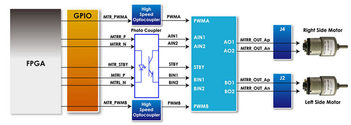
The motor driver board has a motor driver device TB6612FNG, which is responsible for driving motors. The TB6612FNG device provides two channels for output which can control the two motors on the robot simultaneously, each channel provides 1.2A output current, as shown in Figure 4 -25.
The motor driver can receive control signals from the FPGA and provide four control methods for the motor: clockwise(CW) rotation, counterclockwise(CCW) rotation, brake and stop, as shown in Table 4 -6. Note that, there are some photo couplers between the FPGA and TB6612FNG for protection purpose. Therefore, the logic of control signal output from FPGA should be opposite to the logic described in the TB6612FNG datasheet, such us MTRR_P, MTRR_N and MTR_STBY. The only special case is that although MTR_PWMA and MTR_PWMB have passed the photo couplers, but the control logic is not reversed.
The PWM control signal can be up to 100KHz, in our demo, it is set to 7.124KHz. Table 4-7 describes the pin assignments for motor driver TB6612FNG interface.
| FPGA Control Output | Driver Input | Driver
Output
| Modes description | |||||||
| MTRX_P | MTRX_N | MTR_PWMX | MTRX_STBY | IN1 | IN2 | PWM | STBY | O1 | O2 | -- |
| 0 | 0 | 1/0 | 0 | 1 | 1 | 1/0 | 1 | 0 | 0 | Short brake |
| 1 | 0 | 1 | 0 | 0 | 1 | 1 | 1 | 0 | 1 | CCW |
| 0 | 0 | 0 | 1 | 0 | 0 | Short brake | ||||
| 0 | 1 | 1 | 0 | 1 | 0 | 1 | 1 | 1 | 0 | CW |
| 0 | 0 | 0 | 1 | 0 | 0 | Short brake | ||||
| 1 | 1 | 1 | 0 | 0 | 0 | 1 | 1 | OFF
(High Impedance) | Stop | |
| 0/1 | 0/1 | 1/0 | 1 | 1/0 | 1/0 | 1/0 | 0 | OFF
(High Impedance) | Standby | |
| Motor Driver Signal Name | GPIO Pin No. | DE10-Nano FPGA Pin Assignment | Descriptions | Direction for FPGA | I/O Standard |
| MTRR_P | 4 | AH13 | Right Motor Control Signal Input 1 | Output | 3.3-V |
| MTRR_N | 3 | AA19 | Right Motor Control Signal Input 2 | Output | 3.3-V |
| MTRL_P | 5 | W11 | Left Motor Control Signal Input 1 | Output | 3.3-V |
| MTRL_N | 8 | AA18 | Left Motor Control Signal Input 2 | Output | 3.3-V |
| MTR_STBY | 10 | W14 | Standby (Power save) Control Signal | Output | 3.3-V |
| MTR_PWMA | 4 | D11 | Right Motor PWM | Output | 3.3-V |
| MTR_PWMB | 18 | AE24 | Left Motor PWM | Output | 3.3-V |
4-9 DC Motor and Connector
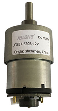
As shown in Figure 4 -26, the motors used on the Self-Balancing Robot are DC deceleration motors. Different from the ordinary motor, the deceleration motor has Speed Reducer which can reduce the rotation speed and increase the torque. After speed reduced, the torque of DC motor is increased, controllability is stronger, Table 4-8 lists the parameters.
| Vender | ASLONG | |
| Part Number | JGB37-520B | |
| Voltage | Workable Range | 6~15V |
| Rated | 12V | |
| No Load | Speed | 333rpm |
| Current | 120ma | |
| Load Torque | Speed | 266rpm |
| Current | 350ma | |
| Torque | 1.14kg.cm | |
| Output | 3W | |
| Stall | Torque | 4.5kg.cm |
| Current | 1ma | |
| Reducer | Ratio | 1:30 |
| Size | 22mm | |
| Weight | 180g | |
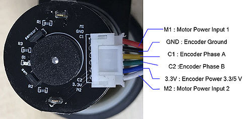
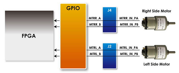
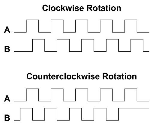
The motor also has two Hall effect sensor and encoder. As shown in Figure 4 -27, the encoder outputs AB-phase square wave to the FPGA(See Figure 4 -28). User can get the rotate speed through the square wave pulse numbers, also can acquire the motor rotate direction through the AB-phase differential, as shown in Figure 4 -29, the motor is forward-rotating when the A-phase is lead ahead of B-phase. User can use these data for balance control. Table 4-9 describes the pin assignments for motor AB-phase signal.
| Motor Encoder Signal Name | GPIO Pin No. | DE10-Nano FPGA Pin Assignment | Descriptions | Direction for FPGA | I/O Standard |
| MTRR_A | 11 | AD5 | The Right Motor Encoder A Signal | Input | 3.3-V |
| MTRR_B | 12 | AG14 | The Right Motor Encoder B Signal | Input | 3.3-V |
| MTRL_A | 13 | AE23 | The Left Motor Encoder A Signal | Input | 3.3-V |
| MTRL_B | 14 | AE6 | The Left Motor Encoder B Signal | Input | 3.3-V |
4-10 Ultrasonic Module
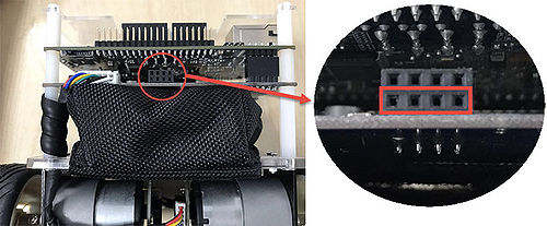
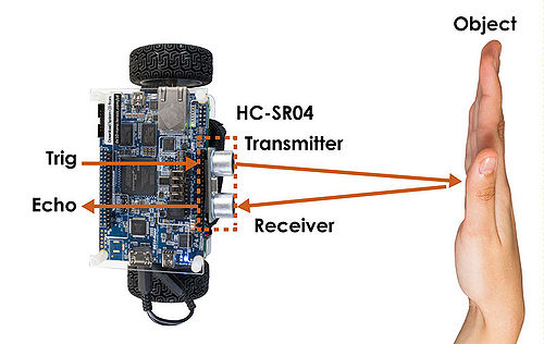
The self-Balancing Robot equips an ultrasonic module interface which can connect with two ultrasonic modules and used to detect the distance of the obstacle in front of the robot, as shown in Figure 4 -30, normally only one module is used. Figure 4-31 shows the default plugin position for the ultrasonic module. The ultrasonic module used on the robot is HC-SR04, when the robot needs to detect the obstacle in front of it, the module emits at least 10us high frequency signal, the module will emit a series of 40KHz sound wave and receive the reflection signal reflected by the nearest obstacle, as shown in Figure 4 -32.
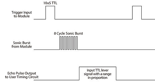
After receiving the reflection signal, Echo pin level will be high, the duration of the high level is the time that the ultrasonic signal is received from the reflection of the obstacle. The distance between the module and obstacle is calculated by formula below. Table 4-10 describes Pin Assignments for Ultrasonic Module, Figure 4-33 shows the Time sequence diagram of the ultrasonic module, Table 4-11 describes the electrical characteristics of the ultrasonic module.
Duration of the high level * sound speed (340M/S)/2
Note: It is divided by 2 in the formula, the reason is that this distance between emission and reflection is twice of the object.
.
| Ultrasonic Module Signal Name | GPIO Pin No. | DE10-Nano FPGA Pin Assignment | Descriptions | Direction for FPGA | I/O Standard |
| TRIG0 | 21 | AC23 | Module Triger Signal 0 | Output | 3.3-V |
| ECHO0 | 22 | AC22 | Module Echo Signal 0 | Input | 3.3-V |
| TRIG1 | 23 | Y19 | Module Triger Signal 1 | Output | 3.3-V |
| ECHO1 | 24 | AB23 | Module Echo Signal 1 | Input | 3.3-V |
| Electrical Characteristics | HC-SR04 Ultrasonic Module |
| Working Voltage | DC 5V |
| Working Current | 15mA |
| Working Frequency | 40Hz |
| Max Range | 4m |
| Min Range | 2cm |
| Measuring Angle | 15 degrees |
| Trigger Input Signal | 10Us TTL pulse |
| Echo Output Signal | Input TTL level signal and the range in proportion |
| Dimension | 45*20*15mm |
4-11 A/D Converter Power Monitor
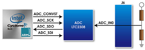
The Self-Balancing Robot reserves a group of resistance as voltage divider circuit, which is used to transmit the battery voltage value to A/D Converter device on DE10-Nano board, the robot can read the battery voltage through FPGA, as shown in Figure 4 -34, Table 4-12 describe the pin assignments for A/D Conveter Power Monitor.
| Signal Name | DE10-Nano FPGA Pin Assignment | Descriptions | Direction for FPGA | I/O Standard |
| ADC_CONVST | U9 | Conversion Start | Output | 3.3-V |
| ADC_SCK | V10 | Serial Data Clock | Output | 3.3-V |
| ASC_SDO | AC4 | Serial Data Input | Input | 3.3-V |
| ADC_SDI | AD4 | Serial Data Out (ADC to FPGA | Output | 3.3-V |
4-12 IR Receiver
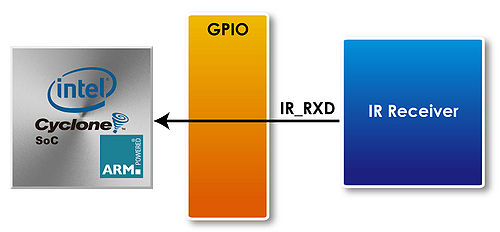
The board comes with an IR remote control receiver module (model: IRM-V538/TR1), the datasheet of this module is provided in the directory \Datasheets\ IR Receiver and Emitter of Balancing Robot system CD. The remote control, which is optional and can be ordered from the website, has an encoding chip (uPD6121G) built-in for generating infrared signals. Figure 4-35 shows the connection of IR receiver to the FPGA. Table 4-13 shows the pin assignment of IR receiver to the FPGA.
| Ultrasonic Module Signal Name | GPIO Pin No. | DE10-Nano FPGA Pin Assignment | Descriptions | Direction for FPGA | I/O Standard |
| IR_RXD | 3 | W11 | IR Receiver | Input | 3.3-V |
Chpater5 Additional Information
Getting Help
Contact us via the following methods for further technical assistance:
- Terasic Inc.9F, No.176, Sec.2, Gongdao 5th Rd, East Dist, Hsinchu City, Taiwan 300-70
- Email : support@terasic.com
- Web : www.terasic.com
| Date | Version | Changes |
| 2018.04.16 | First publication | |
