D5M Resolution Modification
From Terasic Wiki
1.1 Introduction
The design is used to modify the project with the resolution of 800x600 to 1280 x 720 in order to obtain high resolution image captured,large size image, to provide developer more flexible setting of the camera. The whole structure base on the RTL hardware description to devide the project to 5 parts: 1. VGA controller; 2.multi-interface SDRAM controller; 3.RAW to RGB section; 4.CCD capture; 5. D5M Configuration.
1.2 Function Description
- Hardware
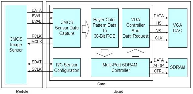
First of all, the CCD camera is being set to be the caputer mode via configure modul,collect the data from the caputer, convert the raw to rgb and store the RGB pixels into buffer. Read the buffer and disply the image in the VGA display to complete the whole procedure of the image capture and display. The diagram1 below reflect the structure:
- Diagram 1 Camera Structure
I2C Sensor Configuration: The modul is being used to set the corresponding function register through the I2C protocols to default the image specification, mothed and the operation on the data captured.
CMOS Sensor Data Capture: the sensor will send out the data by default after the data capture completed, the date is sent out in Line and Frame. If the LVAL is active, the data in line will be sent out with the speed of PCLK.
Muti-Port SDRAM Controller: Through two Write FIFO interface and two Read FIFO interface with the SDRAM controller making up, put the RAW TO RGB data into SDRAM from the Write FIFO interface, then send the data from SDRAM into VGA interface though Read FIFO interface, The FIFO is used to Clock matching and the SDRAM Read & Write controller.
Raw to RGB module:The pixel array which D5M generated has been devided into 2 taps in the Line Buffer, then extract the R, G, B component from the pixel to rebuild the image.
VGA Controller: The VGA controller is used to generate the timing of the VGA interface.
Use the project of DE2_115_CAMERA 800x600 as an example, the user can refer to the instruction below for the concrete paremeters modification.
1. VGA parameter modification Open the VGA_Controller.v file, set the parameter as below for VGA resolution 1280x720 by referring to standard parameter table.
parameter H_SYNC_CYC = 51;
parameter H_SYNC_BACK = 25;
parameter H_SYNC_ACT = 1280;
parameter H_SYNC_FRONT= 20;
parameter H_SYNC_TOTAL= 1376;
// Virtical Parameter ( Line )
parameter V_SYNC_CYC = 2;
parameter V_SYNC_BACK = 11;
parameter V_SYNC_ACT = 720;
parameter V_SYNC_FRONT= 1;
parameter V_SYNC_TOTAL= 734;
Meanwhile, the VGA clock should be set to 60MHz.
Then the VGA parameters have be set as 1028X720p60 now.
What is the procedure for achieving it?
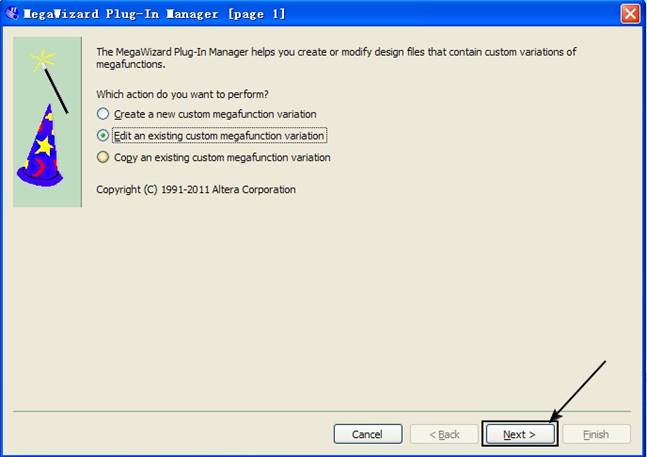
Click Tool > MegaWizard Plug-Manager: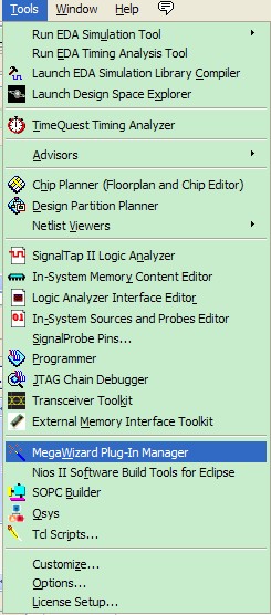
Choose Edit an existing custom megafunction variation, and then click Next.
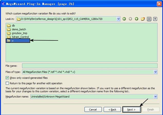
Click the V folder, Next.
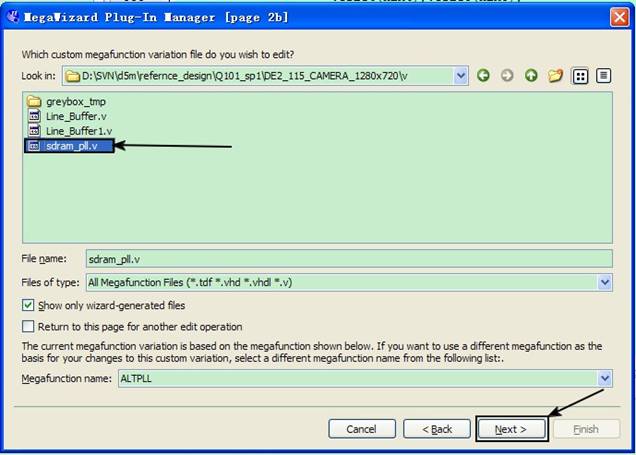
Then choose sdram_pll.v, click Next.
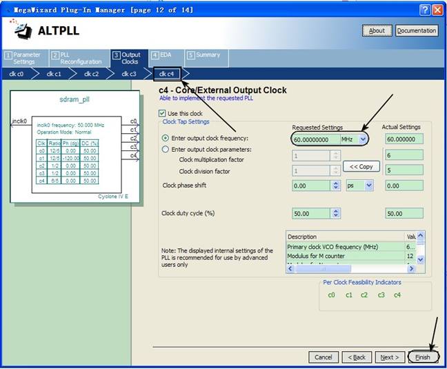
Set clk c4 to 60M, click Finish.
2. The parameters setting for the SDRAM frequency
Update the original 100MHz clk to 120MHz, set the clock phase shift to -125deg (it is optional)
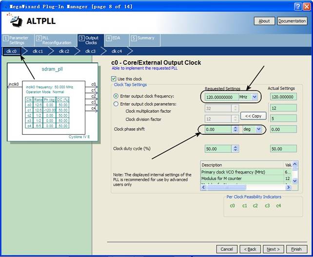
Set the clk c0 to 120MHz in PLL.
Set c1 to 120MHz and clock phase shift to -125deg.
3. Frame buffer setting
After updating the parameters for the resolution, the user needs to modify the width of the Frame Buffer. Open the DE2_115_CAMERA.v file, in the Sdram_Control u7 module, please make the modification:
.WR1_MAX_ADDR(1280*720/2),
.WR2_MAX_ADDR(23'h100000+1280*720/2),
.RD1_MAX_ADDR(1280*720/2),
.RD2_MAX_ADDR(23'h100000+1280*720/2),
Set the parameters of the CCD capture and the Line Buffer. Open the CCD_Capture.v file, and set Parameter COLUMN_WIDTH = 1280; then in the Line_Buffer.v file, make the modification as below: defparam
altshift_taps_component.lpm_hint = "RAM_BLOCK_TYPE=M9K",
altshift_taps_component.lpm_type = "altshift_taps",
altshift_taps_component.number_of_taps = 3,
altshift_taps_component.tap_distance = 1280,
altshift_taps_component.width = 12;
4. Camera Configuration
The user should default a proper width for the Row and Column, then to adjust the pixel frequency to get an unstable image. (1.If the frequency is too high, only high spot can be captured. 2. Should be note the limited of the sdram bandwidth to avoid noise appearance.)
Open I2C_CCD_Config.v file and update:
assign sensor_row_size=24'h03059F;
assign sensor_column_size=24'h0409FF;
assign sensor_row_mode = 24'h220011;
assign sensor_column_mode= 24'h230011;
assign sensor_start_row= 24'h010032;
assign sensor_start_column=24'h020000;
From the parametes modification above, the captured image Specification has been set as 1280X720.
11 : LUT_DATA <= 24'h111A03; // PLL_m_Factor<<8+PLL_n_Divider
12 : LUT_DATA <= 24'h120003; // PLL_p1_Divider
After the modification, the D5M has updated a PLL which can be used to generate the pixel clock internally.Take above parameters as an example, the pixel frequency will be 40.625MHz if the PLL frequency set as 25MHz. (Suggest the user to set a low frequency at the beginning then update the parameters until to get a stable image).
Due to the bandwidth limited of DE2_115SDRAM, there will be come out the niose after these modifications. In order to get the stable output on image, the user needs to reset the H_BALNKING & V_BLANKING values to get accordance of the image output to the image caputer.
3 : LUT_DATA <= 24'h050078; // H_Blanking Legal values: [0, 4095].
4 : LUT_DATA <= 24'h060008; // V_Blanking Legal values: [8, 2047].
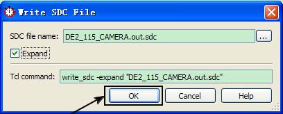
6. Create and add the SDC file.
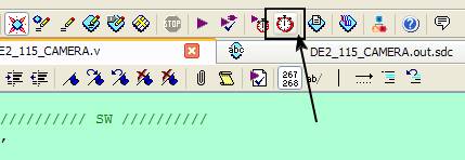
Click timingquest timimg analyzer
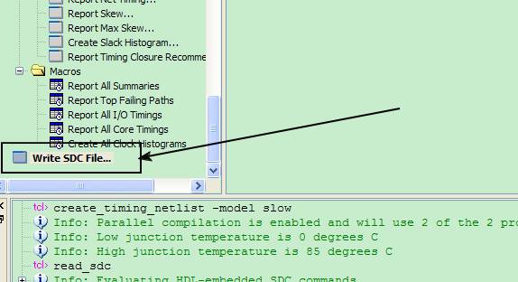
Click WRITE SDC File…
Click OK
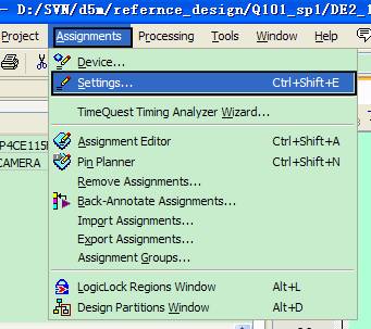
Then Click assignment > setting
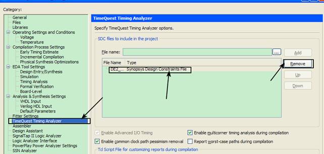
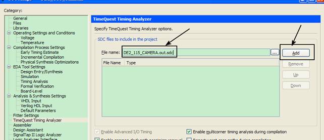
Click the timequest Timing analyzer button, remove the original SDC File and add the new one.
Click apply, then OK Compile the project once again then download.
