DE10-Advance Hardware Manual revC Chapter2
From Terasic Wiki
Chapter 2 Board Components
This chapter provides an introduction to the features and design characteristics of the board.
2.1 Layout and Components
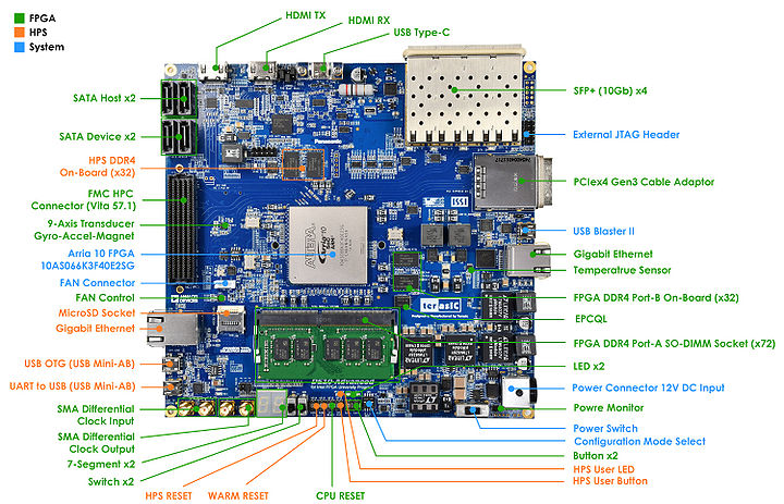
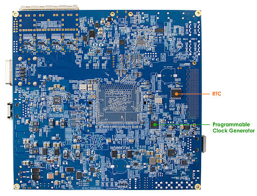
Figure 2-1 and Figure 2-2 shows a photograph of the board. It depicts the layout of the board and indicates the location of the connectors and key components.
- Figure 2-1 DE10-Advanced development board (top view)
- Figure 2-2 DE10-Advanced development board (bottom view)
The DE10-Advanced board has many features that allow users to implement a wide range of designed circuits, from simple circuits to various multimedia projects.
The following hardwares are provided on the board:
- FPGA Device
- Intel ® Arria10® SoC 10AS066K3F40E2SG device (660K LEs)
- USB-Blaster II onboard for programming; JTAG Mode
- Serial configuration device – EPCQL1024
- One DDR4 SO-DIMM Socket, support ECC
- On-board 1GB DDR4-2400, 32-bit data width
- USB Type-C Interface
- Power Delivery
- DisplayPort TX/RX with 4 lanes
- USB 3.0/2.0
- HDMI TX/RX 2.0 for 4K2K@60- FPGA Transceiver
- PCIe Cabling Socket at Gen3 x4
- SFP+ Socket x4, 40Gbps
- SATA 3.0 Host and SATA Device x2 (SATA Connector x4)
- One Gigabit Ethernet Port
- SMA Clock-In and Clock-Out
- High Pin Count FMC Connector. Support VADJ 1.2V/1.5V/1.8V.
- Accelerometer, Gyroscope and Magnetometer
- Temperature Sensor
- Fan Control
- LED x2, KEY x2, Switch x2, 7-Segment x2
- HPS (Hard Processor System)
- 1.5GHz Dual-core ARM Cortex-A9 processor
- Boost Flash Slot:
- 1024 Mb QSPI Flash
- Nand Flash
- MicroSD Socket
- On-board 1GB DDR4-2400, 32-bit data width
- 1 Gigabit Ethernet PHY with RJ45 connector
- USB OTG Port, USB mini-AB connector
- UART to USB, USB Mini-B connector
- RTC
- One user button and one user LED
- Warm reset button and cold reset button
2.2 Block Diagram of the DE10-Advanced Board
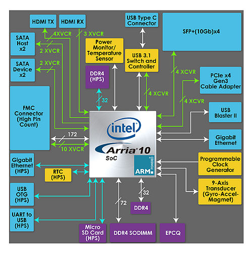
Figure 2-3 is the block diagram of the board. All the connections are established through the Arria 10 SoC FPGA device to provide maximum flexibility for users. Users can configure the FPGA to implement any system design.
- Figure 2-3 Block diagram of DE10-Advanced
Detailed information about Figure 2-3 are listed below.
- Arria 10 SoC 10AS066K3F40E2SG/10AS057K3F40E2SG FPGA
- Dual-core ARM Cortex-A9 (HPS)
- 660K programmable logic elements
- 42,660 Kbits embedded memory
- Hard memory controllers x5
- Transceivers x48(17.4 Gbps)
- 18-bit x 19-bit multipliers x3,356
- Accelerometer & Gyroscope Device MPU9250
- Configuration
- EPCQ1024L Serial Configuration Device
- Onboard USB-Blaster II (Mini-B USB connector)
- Memory Device
- On-board 1GB DDR4-2400, 32-bit data width
- Two DDR4 SO-DIMM SDRAM socket
- Micro SD card socket
- Communication
- USB OTG (Mini-AB USB connector)
- UART-to-USB (Mini-B USB Connector)
- Giga Ethernet x2
- PCIe Gen3 x4 Cabling Socket
- Expansion Ports
- FMC connector
- one HPC(high-pin count) FMC connector with xcvr
- Adjustable VADJ:1.2V/1.5V/1.8V
- FMC connector
- Multimedia Interface
- HDMI TX and RX ports
- Clock
- Two SMA connectors for SMA Clock-In and Clock-Out
- On-board PLLs
- General user input/output
- Buttons x3 (FPGA x2, HPS x1)
- Switches x2 on FPGA
- LEDs x3 (FPGA x2, HPS x1)
- 7-segment displays x2
- System Monitor and Control
- Temperature Sensor on FPGA
- 12V Power Monitor
- Power Controller
- I2C Fan Control
- Power
- 12V DC input


