DE10-Advance Hardware Manual revC Chapter4 PCIe
From Terasic Wiki
4.5 PCIe
The DE10-Advanced board features one PCIe Express downstream interfaces (x4 lane) which are designed to interface with a PC motherboard x4 slot via PCIe cable and PCIe adapter card. Utilizing built-in transceivers on an Arria 10 SoC device, it is able to provide a fully integrated PCI Express-compliant solution for multi-lane (x4) applications. With the PCI Express hard IP block incorporated in the Arria 10 SoC device, it will allow users to implement simple and fast protocols, as well as saving logic resources for logic applications. The PCI Express interface supports complete PCI Express Gen1 at 2.5Gbps/lane, Gen2 at 5.0Gbps/lane, and Gen3 at 8.0Gbps/lane protocol stack solution compliant to PCI Express base specification 3.0 that includes PHY-MAC, Data Link, and transaction layer circuitry embedded in PCI Express hard IP blocks. To use PCIe interface, two external associated devices will be needed to establish a link with PC. First, a PCIe half-height add-in host card with a PCIe x4 cable connector called PCA (PCIe Cabling Adapter Card and See Figure 4-10) will be used to plug into the PCIe slot on a mother board. Then, a PCIe x4 cable (See Figure 4-11) will be used to connect TR5 board and PCIe add-in card as shown in Figure 4-12, the longest length is up to 3 meters. These two associated devices are not included in DE10-Advanced kit. To purchase the PCA card as well as the external cable, please refer to Terasic website pca.terasic.com and PCIe_Cable.terasic.com.
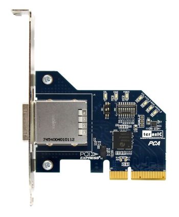
- Figure 4-10 PCIe Cabling Adaptor(PCA) card
_card.jpg)
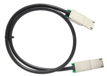
- Figure 4-11 PCIe External Cable

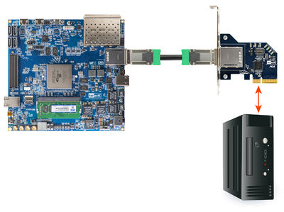
- Figure 4-12 PCIe Link Setup between HAN Pilot Platform and PC

Table 4-8 summarizes the PCI Express pin assignments of the signal names relative to the Arria 10 FPGA.
- Table 4-8 PCI Express pin assignments of the signal names
Schematic Signal Name FPGA Pin Number Description I/O Standard PCIE_REFCLK_p PIN_AH31 PCIe reference clock LVDS PCIE_PREST_n PIN_AW20 PCIe present,active low 1.8V PCIE_WAKE_n PIN_AL19 PCIe wake 1.8V PCIE_TX_p[0] PIN_AR37 PCIe Transmitter data p0 HSSI Differential I/O PCIE_RX_p[0] PIN_AL33 PCIe Receiver data p0 HSSI DIFFERENTIAL I/O PCIE_TX_p[1] PIN_AP39 PCIe Transmitter data p1 HSSI DIFFERENTIAL I/O PCIE_RX_p[1] PIN_AM35 PCIe Receiver data p1 HSSI DIFFERENTIAL I/O PCIE_TX_p[2] PIN_AN37 PCIe Transmitter data p2 HSSI DIFFERENTIAL I/O PCIE_RX_p[2] PIN_AJ33 PCIe Receiver data p2 HSSI Differential I/O PCIE_TX_p[3] PIN_AM39 PCIe Transmitter data p3 HSSI Differential I/O PCIE_RX_p[3] PIN_AK35 PCIe Receiver data p3 HSSI Differential I/O