DE10-Advance Hardware Manual revC Chapter4 User Interface (LED/7-SEG/Button/Switch)
From Terasic Wiki
4.1 User Interface (LED/7-SEG/Button/Switch)
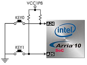
The board has two push-buttons connected to the FPGA, as shown in Figure 4-11. The two push-buttons named KEY0 and KEY1 are connected directly to the Arria 10 SoC FPGA. Table 4-15 list the pin assignment of user push-buttons.
Figure 4-11 Connections between the push-buttons and the Arria 10 SoC FPGA
- Table 4-15 Pin Assignment of Push-buttons
Signal Name FPGA Pin Number Description I/O Standard KEY[0] PIN_A24 Push-button[0] 1.8V KEY[1] PIN_A25 Push-button[1] 1.8V CPU_RESET_n PIN_AN18 CPU_RESET button 1.8V
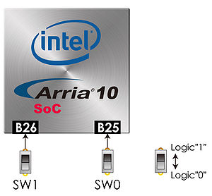
There are two slide switches connected to the FPGA, as shown in Figure 4-12. These switches are not debounced and to be used as level-sensitive data inputs to a circuit. Each switch is connected directly and individually to the FPGA. When the switch is set to the DOWN position (towards the edge of the board), it generates a low logic level to the FPGA. When the switch is set to the UP position, a high logic level is generated to the FPGA. Table 4-16 list the pin assignment of switches.
- Table 4-16 Pin Assignment of Switches
Signal Name FPGA Pin Number Description I/O Standard SW[0] PIN_B25 Slide Switch[0] 1.8 V SW[1] PIN_B26 Slide Switch[1] 1.8 V
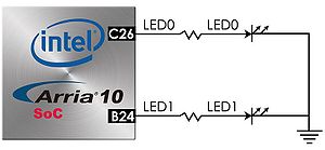
There are also two user-controllable LEDs connected to the FPGA. Each LED is driven directly and individually by the Arria 10 SoC FPGA; driving its associated pin to a high logic level or low level to turn the LED on or off, respectively. Figure 4-13 shows the connections between LEDs and Arria 10 SoC FPGA. Table 4-17 list the pin assignment of LEDs.
- Table 4-17 Pin Assignment of LEDs
Signal Name FPGA Pin Number Description I/O Standard LEDG[0] PIN_C26 LED [0] 1.8 V LEDG[1] PIN_B24 LED [1] 1.8 V
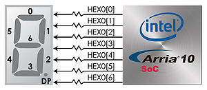
The DE10-Advanced board has two 7-segment displays. These displays are paired to display numbers in various sizes. Figure 4-14 shows the connection of seven segments (common anode) to pins on Arria 10 SoC FPGA. The segment can be turned on or off by applying a low logic level or high logic level from the FPGA, respectively.
Each segment in a display is indexed from 0 to 6, with corresponding positions given in Figure 4-14. Table 4-18 shows the pin assignment of FPGA to the 7-segment displays.
- Table 4-18 Pin Assignment of 7-segment
Signal Name FPGA Pin Number Description I/O Standard HEX0[0] PIN_AT32 Seven Segment Digit 0[0] 1.8V HEX0[1] PIN_AR32 Seven Segment Digit 0[1] 1.8V HEX0[2] PIN_AU32 Seven Segment Digit 0[2] 1.8V HEX0[3] PIN_AU30 Seven Segment Digit 0[3] 1.8V HEX0[4] PIN_AT30 Seven Segment Digit 0[4] 1.8V HEX0[5] PIN_AU29 Seven Segment Digit 0[5] 1.8V HEX0[6] PIN_AV29 Seven Segment Digit 0[6] 1.8V HEX0_DP PIN_AU31 Seven Segment Digit 0_DP 1.8V HEX1[0] PIN_AT28 Seven Segment Digit 1[0] 1.8V HEX1[1] PIN_AT29 Seven Segment Digit 1[1] 1.8V HEX1[2] PIN_AR30 Seven Segment Digit 1[2] 1.8V HEX1[3] PIN_AM27 Seven Segment Digit 1[3] 1.8V HEX1[4] PIN_AL27 Seven Segment Digit 1[4] 1.8V HEX1[5] PIN_AK27 Seven Segment Digit 1[5] 1.8V HEX1[6] PIN_AM26 Seven Segment Digit 1[6] 1.8V HEX1_DP PIN_AR31 Seven Segment Digit 0_DP 1.8V


