DE10-Advance Hardware Manual revC Chapter5 GPIO Header
From Terasic Wiki
5.6 GPIO Header
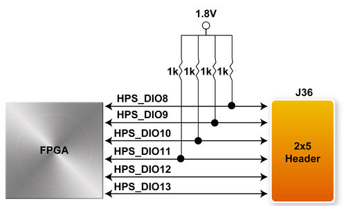
There is a 2x5 pin header(2.54mm) on the DE10-Advanced which connected to six FPGA HPS farbric GPIOs.These I/Os can be used as GPIO that are directly controlled by HPS. Or it can be used as SPI interface (HPS_DIO[11:8]), using the SPI master controller in HPS to communicate with other SPI devices.Table 1-1 shows the pin assignment of the HPS GPIO header.
- Figure 1-1 Connection between FPGA and HPS GPIO Header
- Table 1-1 Pin Assignment of USB OTG PHY
Signal Name FPGA Pin Number Description I/O Standard HPS_DIO8 PIN_D23 HPS GPIO 8; SPIM0_CLK 1.8V HPS_DIO9 PIN_C23 HPS GPIO 9; SPIM0_MISO 1.8V HPS_DIO10 PIN_F23 HPS GPIO 10; SPIM0_CLK 1.8V HPS_DIO11 PIN_G22 HPS GPIO 11; SPIM0_SS0 1.8V HPS_DIO12 PIN_J19 HPS GPIO 12; Reserve 1.8V HPS_DIO13 PIN_L20 HPS GPIO 13; Reserve 1.8V
