DE10-Advance Hardware Manual revC Chapter5 USB OTG
From Terasic Wiki
5.5 USB OTG
The board has one USB 2.0 type-A port with a SMSC USB3320 controller. The SMSC USB3320 device in 32-pin QFN RoHS Compliant package. This device supports UTMI+ Low Pin Interface (ULPI), which communicates with the USB 2.0 controller in HPS. The PHY operates in Host mode by connecting the ID pin of USB3320 to ground. When operating in Host mode, the device is powered by the USB type-A port. Figure 5-4 shows the connections of USB PTG PHY to the HPS. Table 5-6 lists the pin assignment of USB OTG PHY to the HPS.
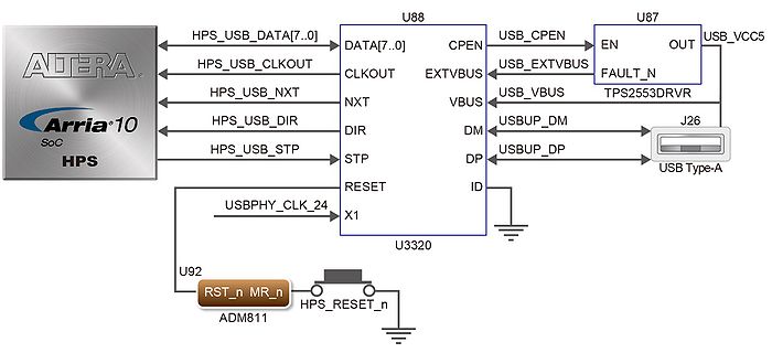
- Figure 5-4 Connections between the HPS and USB OTG PHY

- Table 5-6 Pin Assignment of USB OTG PHY
Signal Name FPGA Pin Number Description I/O Standard HPS_USB_CLKOUT PIN_L25 60MHz Reference Clock Output 1.8V HPS_USB_DATA[0] PIN_K25 HPS USB_DATA[0] 1.8V HPS_USB_DATA[1] PIN_G26 HPS USB_DATA[1] 1.8V HPS_USB_DATA[2] PIN_E27 HPS USB_DATA[2] 1.8V HPS_USB_DATA[3] PIN_F27 HPS USB_DATA[3] 1.8V HPS_USB_DATA[4] PIN_L24 HPS USB_DATA[4] 1.8V HPS_USB_DATA[5] PIN_M24 HPS USB_DATA[5] 1.8V HPS_USB_DATA[6] PIN_K23 HPS USB_DATA[6] 1.8V HPS_USB_DATA[7] PIN_L23 HPS USB_DATA[7] 1.8V HPS_USB_DIR PIN_J25 Direction of the Data Bus 1.8V HPS_USB_NXT PIN_H26 Direction of the Data Bus 1.8V HPS_USB_STP PIN_M25 Stop Data Stream on the Bus 1.8V