DE10-Advance Hardware Manual revC Chapter8 General Design Flow
From Terasic Wiki
8.2 General Design Flow
This section will introduce the general design flow to build a project for the FPGA board via the System Builder. The general design flow is illustrated in the Figure 8-1.
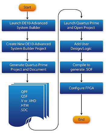
- Figure 8-1 The general design flow of building a project
- Figure 8-1 The general design flow of building a project

Users should launch System Builder and create a new project according to their design requirements. When users complete the settings, the System Builder will generate two major files which include top-level design file (.v) and the Quartus Prime setting file(.qsf).
The top-level design file contains top-level Verilog wrapper for users to add their own design/logic. The Quartus Prime setting file contains information such as FPGA device type, top-level pin assignment, and I/O standard for each user-defined I/O pin.
Finally, Quartus Prime programmer must be used to download SOF file to the FPGA board using JTAG interface.