DE10-Advance Hardware Manual revC Chapter8 Using DE10-Advanced System Builder
From Terasic Wiki
Contents |
8.3 Using DE10-Advanced System Builder
This section provides the detailed procedures on how to use the DE10-Advanced System Builder.
8.3.1 Install and Launch the DE10-Advanced System Builder
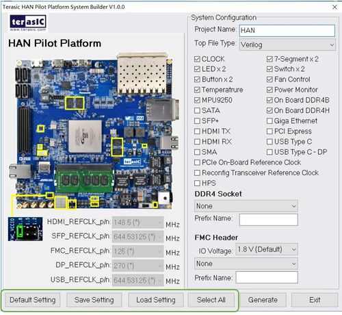
The DE10-Advanced System Builder is located in the directory: “Tools\SystemBuilder” of the DE10-Advanced System CD. Users can copy the entire folder to a host computer without installing the utility. A window will pop up, as shown in Figure 8-2, after executing the DE10-Advanced SystemBuilder.exe on the host computer.
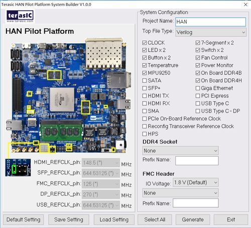
- Figure 8-2 The GUI of DE10-Advanced System Builder

8.3.2 Enter Project Name
Enter the project name in the circled area, as shown in Figure 8-3. The project name typed in will be assigned automatically as the name of your top-level design entity.
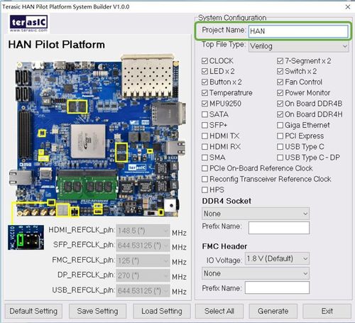
- Figure 8-3 Project Name in the System Builder window

8.3.3 Select Top File Type
The system builder can generate Verilog or VHDL Quartus top file according to users’requirement. Users can select their desired file type in the Top File Type list-box shown in Figure 8-4.

- Figure 8-4 Top File Type in the System Builder window

8.3.4 System Configuration
Users are given the flexibility of enabling their choices of components connected to the FPGA under System Configuration, as shown in Figure 8-5. Each component of the FPGA board is listed to be enabled or disabled according to users’ needs. If a component is enabled, the System Builder will automatically generate the associated pin assignments including its pin name, pin location, pin direction, and I/O standards. Note: The pin assignments for some components (e.g. DDR4 and SFP+) require associated controller codes in the Quartus project or it would result in compilation error. Hence please do not select them if they are not needed in the design.
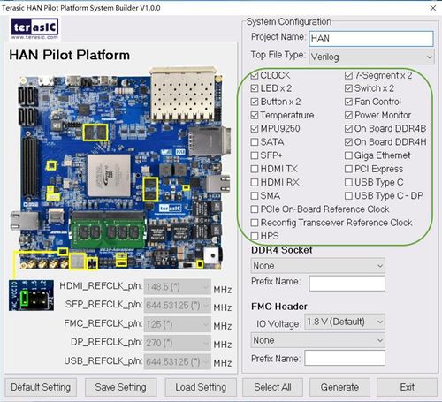
- Figure 8-5 System Configuration group

8.3.5 FMC Expansion
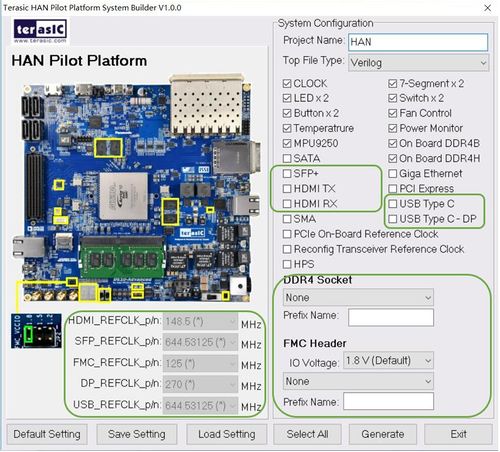
If users connect any compatible Terasic FMC-based daughter cards to the FMC connectoron DE10-Advanced, the DE10-Advanced System Builder can generate a project that include the corresponding module, as shown in Figure 8-6. It will also generate the associated pin assignment automatically, including pin name, pin location, pin direction, and I/O standard.
The “Prefix Name” is an optional feature that denotes the pin name of the daughter card assigned in your design. Users may leave this field blank.

- Figure 8-6 FMC expansion group

8.3.6 Programmable Clock Generator
There are some oscillators on-board (Si5350C,CDCM6208) that provide reference clocks for the following signals:
- HDMI_REFCLK
- SFP_REFCLK
- FMC_REFCLK
- DP_REFCLK
- USB_REFCLK
To use these clock, users can select the desired frequency on the Programmable Oscillator group, as shown in Figure 8-7. DDR4, or SFP+ must be checked before users can start to specify the desired frequency in the programmable oscillators. As the Quartus project is created, System Builder automatically generates the associated controller according to users’ desired frequency in Verilog which facilitates users’ implementation as no additional control code is required to configure the programmable oscillator.
Note: If users need to dynamically change the frequency, they would need to modify the generated control code themselves.
- Figure 8-7 External programmable oscillators

8.3.7 Project Setting Management
The System Builder also provides functions to restore default setting, load a setting, and save board configuration file, as shown in Figure 8-8. Users can save the current board configuration information into a .cfg file and load it into the System Builder.
- Figure 8-8 Project Settings

8.3.8 Project Generation
When users press the Generate button, the DE10-Advanced System Builder will generate the corresponding Quartus Prime files and documents as listed in Table 8‑1.
- Table 8-1 The file generated by DE10-Advanced System Builder
No. File Name Descriptions 1 <Project name>.v Top Verilog Quartus Prime File 2 <Project name>.qpf Quartus Prime Project File 3 <Project name>.qsf Quartus Prime Setting File 4 <Project name>.sdc Quartus Prime Synopsis Design Constraints File 5 <Project name>.htm Pin Assignment Document
Users can use Quartus Prime software to add custom logic into the project and compile the project to generate the SRAM Object File. (.sof).