DE10-Advance usermanual revB
From Terasic Wiki
Chapter 1 DE10-Advanced Development Kit
The DE10-Advanced Development Kit provides users a combination of ARM software and FPGA hardware development platforms. It has a vast memory device and peripherals on the hardware. This kit also includes resourceful reference designs to help users to accomplish their design needs. The hardware offers in the DE10-Advanced has the maximum capacity with 660K Les in Arria 10 SoC FPGA and featuring various types of high-speed image interface such as: HDMI, Display Port, and 12G-SDI and a large capacity of DDR4 memory. The board’s high speed network interface, Gigabit Ethernet and SFP+10GbE, provides hardware resources for network communications related applications.
The HPS can be reboot with any of these three removable daughter cards: MicroSD Card, Nand Flash, and QSPI Flash. The FPGA on the main board can be connected to DDR4-SODIMM Socket in addition to the DDR4 memory module. The FPGA on the main board can also be connected to the Terasic QDR Memory Module as well. Beside the DDR4 memory module, you can also directly connect to the FPGA on the main board via the High Pin Count FMC expansion port to expand variety of functions.
The PCIe Gen3 x4 Connector interface comes with the Terasic PCA PCIe and PCIe Cable, which can be used to connect the Host PC to allow data between the FPGA and the Host PC. The USB Type-C interface on the motherboard allows the motherboard to obtain power for the host PC. The Host PC displays information and images through the high-speed transmission USB 3.0 or the Display Port.
1.1 Package Contents

- DE10-Advanced SoC FPGA Development Kit
- MicroSD Card (Installed)
- Fan (Installed)
- Two Type A to Mini-B USB Cables
- 12V DC Power Supply (Installed)
- AC Power Cord (USA)
- One 4GB DDR4 ECC SO-DIMM Module (Installed)
- Screws, Copper Stands, and Silicon Footstands
1.2 DE10-Advanced System CD
The DE10-Advanced System CD contains all the documents and supporting materials associated with DE10-Advanced, including the user manual, system builder, reference designs and device datasheets. Users can download this system CD from the link: http://DE10-Advanced.terasic.com/cd.
1.3 Getting Help
- Here are the addresses where you can get help if you encounter any problems:
- Terasic Technologies
- 9F., No.176, Sec.2, Gongdao 5th Rd, East Dist, Hsinchu City, 30070. Taiwan
- Email: support@terasic.com
- Tel.: +886-3-575-0880
- Website: DE10-Advanced.terasic.com
Chapter 2 Introduction of the DE10-Advanced Board
This chapter provides an introduction to the features and design characteristics of the board.
2.1 Layout and Components
Figure 2-1 and Figure 2-2 shows a photograph of the board. It depicts the layout of the board and indicates the location of the connectors and key components.

- Figure 2-1 DE10-Advanced development board (top view)

- Figure 2-2 DE10-Advanced development board (bottom view)
The DE10-Advanced board has many features that allow users to implement a wide range of designed circuits, from simple circuits to various multimedia projects.
The following hardwares are provided on the board:
- FPGA Device
- Intel ® Arria10® SoC 10AS066K3F40E2SG device (660K LEs)
- USB-Blaster II onboard for programming; JTAG Mode
- Serial configuration device – EPCQL1024
- One DDR4 SO-DIMM Socket, support ECC
- On-board 1GB DDR4-2400, 32-bit data width
- USB Type-C Interface
- Power Delivery
- DisplayPort TX/RX with 4 lanes
- USB 3.0/2.0
- HDMI TX/RX 2.0 for 4K2K@60- FPGA Transceiver
- PCIe Cabling Socket at Gen3 x4
- SFP+ Socket x4, 40Gbps
- SATA 3.0 Host and SATA Device x2 (SATA Connector x4)
- One Gigabit Ethernet Port
- SMA Clock-In and Clock-Out
- High Pin Count FMC Connector. Support VADJ 1.2V/1.5V/1.8V.
- Accelerometer, Gyroscope and Magnetometer
- Temperature Sensor
- Fan Control
- LED x2, KEY x2, Switch x2, 7-Segment x2
- HPS (Hard Processor System)
- 1.5GHz Dual-core ARM Cortex-A9 processor
- Boost Flash Slot:
- 1024 Mb QSPI Flash
- Nand Flash
- MicroSD Socket
- On-board 1GB DDR4-2400, 32-bit data width
- 1 Gigabit Ethernet PHY with RJ45 connector
- USB OTG Port, USB mini-AB connector
- UART to USB, USB Mini-B connector
- RTC
- One user button and one user LED
- Warm reset button and cold reset button
2.2 Block Diagram of the DE10-Advanced Board
Figure 2-3 is the block diagram of the board. All the connections are established through the Arria 10 SoC FPGA device to provide maximum flexibility for users. Users can configure the FPGA to implement any system design.

- Figure 2-3 Block diagram of DE10-Advanced
Detailed information about Figure 2-3 are listed below.
- Arria 10 SoC 10AS066K3F40E2SG/10AS057K3F40E2SG FPGA
- Dual-core ARM Cortex-A9 (HPS)
- 660K programmable logic elements
- 42,660 Kbits embedded memory
- Hard memory controllers x5
- Transceivers x48(17.4 Gbps)
- 18-bit x 19-bit multipliers x3,356
- Accelerometer & Gyroscope Device MPU9250
- Configuration
- EPCQ1024L Serial Configuration Device
- Onboard USB-Blaster II (Mini-B USB connector)
- Memory Device
- On-board 1GB DDR4-2400, 32-bit data width
- Two DDR4 SO-DIMM SDRAM socket
- Micro SD card socket
- Communication
- USB OTG (Mini-AB USB connector)
- UART-to-USB (Mini-B USB Connector)
- Giga Ethernet x2
- PCIe Gen3 x4 Cabling Socket
- Expansion Ports
- FMC connector
- one HPC(high-pin count) FMC connector with xcvr
- Adjustable VADJ:1.2V/1.5V/1.8V
- FMC connector
- Multimedia Interface
- HDMI TX and RX ports
- Clock
- Two SMA connectors for SMA Clock-In and Clock-Out
- On-board PLLs
- General user input/output
- Buttons x3 (FPGA x2, HPS x1)
- Switches x2 on FPGA
- LEDs x3 (FPGA x2, HPS x1)
- 7-segment displays x2
- System Monitor and Control
- Temperature Sensor on FPGA
- 12V Power Monitor
- Power Controller
- I2C Fan Control
- Power
- 12V DC input
3 Chapter 3 Board Setting and Status component
This chapter describes all the setting devices on DE10-Advanced board and their functions, such as Switches and Headers. We also will describe the function of some status LEDs. The JTAG interface will be described at the end of this chapter.
3.1 Board Setting Switches
- Mode Select Switches
Mode Select Switch(SW5) is used to set the DE10-Advanced FPGA MSEL pin value.These MSEL pins determined the Configuration Mode of the FPGA.Table 3-1 list the MSEL setting for configuration scheme of FPGA,when MSEL is set to AS mode(Factory default setting),FPGA will be booted from EPCQ device(See Figure 3-1).When MSEL is set to FPP mode(See Figure 3-2),FPGA can be configured by HPS Fabric(From Micro SD Card).
- Table 3-1 MSEL setting for configuration scheme of FPGA
Configuration Scheme SW5 MSEL[2..0] Setting Description AS Mode (Factory Default) 010 FPGA boot from EPCQ FPP Mode 001 FPGA boot from Micro SD Card

- Figure 3-1 The AS mode setting of SW5

- Figure 3-2 The FPP mode setting of SW5
3.2 Board Setting Headers
- JTAG Interface Header
J17 is the header used to set the JTAG bus of FMC connector connect to JTAG interface of DE10-Advanced system.The FMC connector will not be included in the JTAG chain if the headers are set to open(See Figure 3-3). Table 3-2 list the setting of the J17 header.
- Table 3-2 JTAG Interface Headers Setting
Header Setting Descriptions J17 Open (Default Setting) Disable the JTAG interface of the FMC connector into the JTAG chain

- Figure 3-3 The FMC Jtag Header
- FMC_VCCIO Select Header
JP2 is used to set the VCCIO voltage of FPGA I/O on FMC connector, as1.2V/1.5V/1.8V are supported, the FMC connector can support various I/0 standard FMC daughtercards. Table 3-3 list the FMC_VCCIO Headers Setting.
- Table 3-3 FMC_VCCIO Headers Setting
JP2 Setting FMC VCCIO Voltage 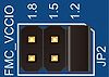
1.2V 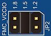
1.5V 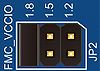
1.8V(Default Setting)


- Figure 3-4 The FMC VCCIO select header
- PMODE Select Header
The USB 3.0 Controller (Cypress FX3) on the DE10-Advanced can be booted from a different sources, selected by the configuration of the PMODE header(JP4/JP5/JP6) on DE10-Advanced. Table 3-4 shows the boot options and associated settings. The default boot device is the from an serial flash via SPI interface.
- Table 3-4 PMODE Headers Setting
PMODE[2:0](JP6/JP5/JP4) Setting Boot Source F00 Sync ADMux (16-bit) F01 Async ADMux (16-bit) F11 USB boot F0F Async SRAM (16-bit) F1F I2C, On Failure, USB Boot is Enabled 1FF I2C only 0F1(Defualt) SPI, On Failure, USB Boot is Enabled
- F indicates Floating

- Figure 3-5 The PMODE select header
3.3 Status LED
This section describes the all status LED for the interfaces on DE10-Advanced board. Figure 3-6 shows all the status LED on the DE10-advanced. Following are the detailed descriptions of these interface LED.

- Figure 3-6 The status LED on the DE10-Advanced board
- UART Interface
- Table 3-5 list the two status LEDs for UART interface.
- Table 3-5 Status LED for UART Interface
Component Reference Status Descriptions TXD1 UART_TXD ON Transmitting RXD1 UART_RXD ON Receiving
- SFP Interface
- Table 3-6 list the four status LEDs for SFP interface.
- Table 3-6 Indicator LED for SFP Interface
Component Reference Status Descriptions D4 SFPA_MOD0_PRSNT_n ON Indicate that the SFP module is present on the SFPA D3 SFPB_MOD0_PRSNT_n ON Indicate that the SFP module is present on the SFPB D2 SFPC_MOD0_PRSNT_n ON Indicate that the SFP module is present on the SFPC D1 SFPD_MOD0_PRSNT_n ON Indicate that the SFP module is present on the SFPD
- Ethernet Interface
- Table 3-7 list the four status LEDs for Ethernet interface.
- Table 3-7 Status LED for Ethernet Interface
Component Reference Status Descriptions D8 ETH_LED_TX ON Transmitting D9 ETH_LED_RX ON Receiving D10 ETH_LINK1000 ON 1000Mbps Link UP D11 ETH_LINK100 ON 100Mbps Link UP
- Power
- Table 3-8 list the two status LEDs for power.
- Table 3-8 Status LED for Power
Component Reference Status Descriptions D31 12V~20V Power Indicator ON Illuminates when 12V~20V power Power Supply is active
- USB Blaster
- Table 3-6 list the two status LEDs for USB Blaster interface.
- Table 3-5 Status LED for USB Blaster Interface
Component Reference Status Descriptions D5 JTAG_TX ON Illuminates when JTAG interface is transmitting data D6 JTAG_RX ON Illuminates when JTAG interface is receiving data
3.4 JTAG Interface
Figure 3-2 shows the JTAG interface of DE10-Advanced.Users can access to the JTAG interface through the USB Blaster II circuit or connect external blaster to external blaster header.All the devices which implement JTAG are connect to MAX II device,and switch via MAX II internal switch logic.By using headers J17,users can include FMC connector JTAG interface in the DE10-Advanced JTAG Chain,or exclude them from the JTAG Chain.The default JTAG path for de10-advanced is: USB Blaster II ==> HPS ==> FPGA ==> (Bypass FMC connector) ==> USB Blaster II.When the External JTAG connector is connected to the external blaster, the On board's USB blaster II function will be replaced by the external blaster.

- Figure 3-2 JTAG interface of DE10-Advanced
Chapter 4 FPGA Fabric component
4.1 USB Type C Port
The DE10-Advanced board features one USB Type C connector. It is designed for high-speed data transmission with computers and image output applications. Figure 4-1 shows the block diagram of the connection between USB Type C port and FPGA.
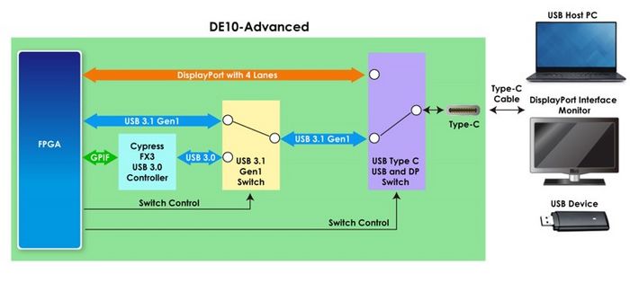
- Figure 4-1 Block diagram of the connection between USB Type C port and FPGA

As shown in Figure 4-1, it connects to FPGA through several switch circuits and USB controllers, users can switch USB Type C connector to a variety of applications as below:
- USB 3.0 Device to USB Host PC
- USB 2.0 OTG
- DisplayPort Source Application (Need DP Source IP)
- USB 3.1 Gen1 Application (Need USB 3.1 Gen1 IP)
We will describe the circuits diagram and these functions in detail below.
4.1.1 Display Port
As shown in Figure 3-2,USB type C port can connect to FPGA transceiver. Users can implement a Display port source mode IP in FPGA, the DE10-Advanced board will implement the features of display port source.
Through the USB Type C cable, users can connect DE10-Advanced board to the monitor which supports Display port interface. Then the image processed by FPGA can be displayed on the monitor.
Th display port provides data rate up to 5.4Gbps per lane and 4 lanes in total, it supports DisplayPort 1.2a Spec.
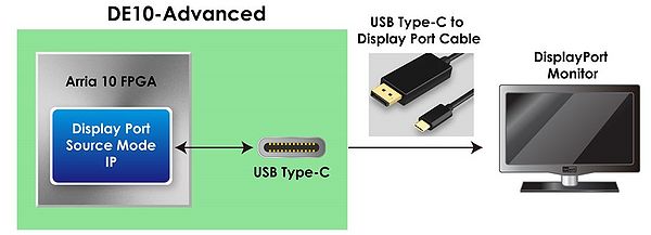
- Figure 4-2 USB Type-C Application : DisplayPort TX Source

- Table 4-1 DisplayPort Signal Names and Functions
Signal Name FPGA Pin Number Description I/O Standard DP_REFCLK_p AM31 Display reference clock form PLL LVDS DP_TX_p[0] AW37 TX Lane 1 HSSI Differential I/O DP_TX_p[1] AV39 TX Lane 2 HSSI Differential I/O DP_TX_p[2] AU37 TX Lane 3 HSSI Differential I/O DP_TX_p[3] AT39 TX Lane 4 HSSI Differential I/O DP_AUX_p AM22 Display port AUX port DIFFERENTIAL 1.8-V SSTL CLASS I DP_DX_SEL AB27 Display Port channel TX or RX(Reserve) select.
DP_DX_SEL = 0 : USB TypeC in Display TX mode .
DP_DX_SEL = 1(Reserve) : USB TypeC in Display RX mode1.8 V DP_AUX_SEL AC28 AUX/DDC Selection Control Pin in Conjunction with Dx_SEL Pin 1.8 V
4.1.2 USB 3.0 Device
The DE10-Advanced board has one Cypress FX3 USB Controller(CYUSB3014).The USB controller is connected to FPGA through the programmable GPIF II interface, and connect to the external USB Type C connector, It provides USB 3.0 Device application for DE10-Advanced board.
As shown in Figure 4-3, users can connect FX3 USB Controller to PC through USB Type C cable, and transfer USB 3.0 data between FPGA and USB Host PC with transfer rate 320MByte/s (Using the demonstration provided by Cypress).
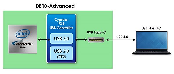
- Figure 4-3 FX3 USB 3.0 Controller application

4.1.3 USB 2.0 OTG
The Cypress FX3 USB controller also has a USB 2.0 OTG controller. It allows the DE10-Advanced board function as an OTG Host to MSC as well as HID-class devices, as shown in Figure 4-4.
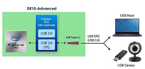
- Figure 4-4 USB 2.0 OTG Controller application

- Table 4-2 FX3 USB 3.0 Controller Signal Names and Functions
| Signal Name | FPGA Pin Number | Description | I/O Standard |
|---|---|---|---|
| USBFX3_DQ[0] | AU21 | GPIF II Data Bus 0 | 1.8 V |
| USBFX3_DQ[1] | AW23 | GPIF II Data Bus 1 | 1.8 V |
| USBFX3_DQ[2] | AW24 | GPIF II Data Bus 2 | 1.8 V |
| USBFX3_DQ[3] | AW25 | GPIF II Data Bus 3 | 1.8 V |
| USBFX3_DQ[4] | AW26 | GPIF II Data Bus 4 | 1.8 V |
| USBFX3_DQ[5] | AV24 | GPIF II Data Bus 5 | 1.8 V |
| USBFX3_DQ[6] | AW28 | GPIF II Data Bus 6 | 1.8 V |
| USBFX3_DQ[7] | AW30 | GPIF II Data Bus 7 | 1.8 V |
| USBFX3_DQ[8] | AW29 | GPIF II Data Bus 8 | 1.8 V |
| USBFX3_DQ[9] | AV27 | GPIF II Data Bus 9 | 1.8 V |
| USBFX3_DQ[10] | AV28 | GPIF II Data Bus 10 | 1.8 V |
| USBFX3_DQ[11] | AU26 | GPIF II Data Bus 11 | 1.8 V |
| USBFX3_DQ[12] | AV23 | GPIF II Data Bus 12 | 1.8 V |
| USBFX3_DQ[13] | AU25 | GPIF II Data Bus 13 | 1.8 V |
| USBFX3_DQ[14] | AR25 | GPIF II Data Bus 14 | 1.8 V |
| USBFX3_DQ[15] | AP24 | GPIF II Data Bus 15 | 1.8 V |
| USBFX3_DQ[16] | AL23 | GPIF II Data Bus 16 | 1.8 V |
| USBFX3_DQ[17] | AM24 | GPIF II Data Bus 17 | 1.8 V |
| USBFX3_DQ[18] | AK25 | GPIF II Data Bus 18 | 1.8 V |
| USBFX3_DQ[19] | AM25 | GPIF II Data Bus 19 | 1.8 V |
| USBFX3_DQ[20] | AT24 | GPIF II Data Bus 20 | 1.8 V |
| USBFX3_DQ[21] | AR26 | GPIF II Data Bus 21 | 1.8 V |
| USBFX3_DQ[22] | AP26 | GPIF II Data Bus 22 | 1.8 V |
| USBFX3_DQ[23] | AP25 | GPIF II Data Bus 23 | 1.8 V |
| USBFX3_DQ[24] | AN24 | GPIF II Data Bus 24 | 1.8 V |
| USBFX3_DQ[25] | AN26 | GPIF II Data Bus 25 | 1.8 V |
| USBFX3_DQ[26] | AK23 | GPIF II Data Bus 26 | 1.8 V |
| USBFX3_DQ[27] | AJ25 | GPIF II Data Bus 27 | 1.8 V |
| USBFX3_DQ[28] | AJ23 | GPIF II Data Bus 28 | 1.8 V |
| USBFX3_DQ[29] | AH23 | GPIF II Data Bus 29 | 1.8 V |
| USBFX3_DQ[30] | AR20 | GPIF II Data Bus 30 | 1.8 V |
| USBFX3_DQ[31] | AP20 | GPIF II Data Bus 31 | 1.8 V |
| USBFX3_CTL0_SLCS_n | AV26 | GPIF II Control Bus 0 | 1.8 V |
| USBFX3_CTL1_SLWR_n | AT22 | GPIF II Control Bus 1 | 1.8 V |
| USBFX3_CTL2_SLOE_n | AT25 | GPIF II Control Bus 2 | 1.8 V |
| USBFX3_CTL3_SLRD_n | AR27 | GPIF II Control Bus 3 | 1.8 V |
| USBFX3_CTL4_FLAGA | AN22 | GPIF II Control Bus 4 | 1.8 V |
| USBFX3_CTL5_FLAGB | AN23 | GPIF II Control Bus 5 | 1.8 V |
| USBFX3_CTL6 | AL24 | GPIF II Control Bus 6 | 1.8 V |
| USBFX3_CTL7_PKTEND_n | AL25 | GPIF II Control Bus 7 | 1.8 V |
| USBFX3_CTL8 | AV21 | GPIF II Control Bus 8 | 1.8 V |
| USBFX3_CTL9 | AV22 | GPIF II Control Bus 9 | 1.8 V |
| USBFX3_CTL10 | AU24 | GPIF II Control Bus 10 | 1.8 V |
| USBFX3_CTL11_A1 | AU22 | GPIF II Control Bus 11 | 1.8 V |
| USBFX3_CTL12_A0 | AT23 | GPIF II Control Bus 12 | 1.8 V |
| USBFX3_CTL15_INT_n | AW21 | GPIF II Control Bus 15 | 1.8 V |
| USBFX3_RESET_n | AJ24 | FX3 reset | 1.8 V |
| USBFX3_PCLK | AT27 | FX3 clok | 1.8 V |
| USBFX3_UART_TX | AP23 | USB to UART transmitter | 1.8 V |
| USBFX3_UART_RX | AU27 | USB to UART receiver | 1.8 V |
| USBFX3_OTG_ID | AG26 | OTG ID pin | 1.8 V |
4.1.4 USB 3.1 Gen1 Application
As shown in Figure 4-5, user can implement an independent or a third-party USB 3.1 Host or Device IP in FPGA. Through the circuit of FPGA and USB type C connector, the FPGA transceiver can connect to USB Type C connector and achieve the USB 3.o or USB 3.1 Host or Device application.
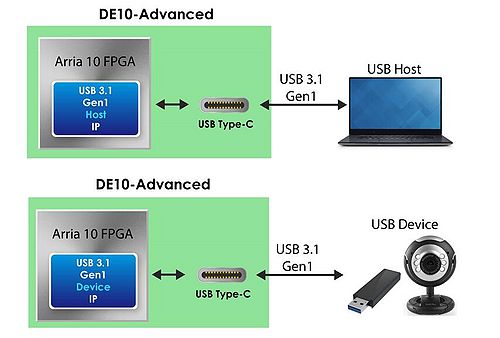
- Figure 4-5 Using USB 3.1 Gen 1 IP

- Table 4-3 USB 3.1 Gen 1 application Signal Names and Functions
Signal Name FPGA Pin Number Description I/O Standard USB_REFCLK_p AB31 USB usb reference clock LVDS USB_TX_p AB39 USB 3.1 Interface transmitter line HSSI Differential I/O USB_RX_p AA37 USB 3.1 Interface receiver line HSSI Differential I/O
4.1.5 Power Application
The DE10-Advanced board also can be powered through USB Type C port with USB Type C power adpater. The adapter with power above 80W is recommended for DE10-Advanced board.
Note: Make sure the USB to UART connector (J27) is not connected before using the power adapter, or the DE10-Advanced board can't be power on normally. User can use J27 after the board is powered on.
4.2 Display Port
4.3 SFP+ Connector
The development board has four independent 10G SFP+ connectors that use one transceiver channel each from the Arria 10 SoC FPGA device. These modules take in serial data from the Arria 10 SoC FPGA device and transform them to optical signals. The board includes cage assemblies for the SFP+ connectors.Figure 4-3 shows the connections between the SFP+ and Arria 10 SoC FPGA.
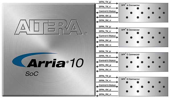
- Figure 4-3 Connection between the SFP+ and Arria 10 SoC FPGA
- Figure 4-3 Connection between the SFP+ and Arria 10 SoC FPGA

Table 4-3, Table 4-4, Table 4-5 and Table 4-6 list the four QSF+ connectors assignments and signal names relative to the Arria 10 SoC FPGA
- Table 4-3 SFP+ A Pin Assignments, Signal Names and Functions
Signal Name FPGA Pin Number Description I/O Standard SFPA_TXDISABLE PIN_AR28 Turns off and disables the transmitter output 1.2V SFPA_TXFAULT PIN_AP28 Transmitter fault 1.2V SFPA_TX_p PIN_AG37 Transmiter data HSSI DIFFERENTIAL I/O SFPA_RX_p PIN_AD35 Receiver data HSSI DIFFERENTIAL I/O SFPA_LOS PIN_AN6 Signal loss indicator 1.2V SFPA_MOD0_PRSNT_n PIN_AU4 Module present 1.2V SFPA_RATESEL0 PIN_AM19 Rate select 0 3.3V SFPA_RATESEL1 PIN_AN17 Rate select 1 3.3V SFPA_TX_n PIN_AG36 Transmitter data HSSI DIFFERENTIAL I/O SFPA_RX_n PIN_AD34 Receiver data HSSI DIFFERENTIAL I/O
- Table 4-4 SFP+ B Pin Assignments, Signal Names and Functions
Signal Name FPGA Pin Number Description I/O Standard SFPB_TXDISABLE PIN_AU5 Turns off and disables the transmitter output 1.2V SFPB_TXFAULT PIN_AE10 Transmitter fault 1.2V SFPB_TX_p PIN_AF39 Transmiter data HSSI DIFFERENTIAL I/O SFPB_RX_p PIN_AC37 Receiver data HSSI DIFFERENTIAL I/O SFPB_LOS PIN_AN12 Signal loss indicator 1.2V SFPB_MOD0_PRSNT_n PIN_AT5 Module present 1.2V SFPB_RATESEL0 PIN_AR18 Rate select 0 3.3V SFPB_RATESEL1 PIN_AP18 Rate select 1 3.3V SFPB_TX_n PIN_AF38 Transmitter data HSSI DIFFERENTIAL I/O SFPB_RX_n PIN_AC36 Receiver data HSSI DIFFERENTIAL I/O
- Table 4-5 SFP+ C Pin Assignments, Signal Names and Functions
Signal Name FPGA Pin Number Description I/O Standard SFPC_TXDISABLE PIN_AP30 Turns off and disables the transmitter output 1.2V SFPC_TXFAULT PIN_AP28 Transmitter fault 1.2V SFPC_TX_p PIN_AE37 Transmiter data HSSI DIFFERENTIAL I/O SFPC_RX_p PIN_AC33 Receiver data HSSI DIFFERENTIAL I/O SFPC_LOS PIN_AN28 Signal loss indicator 1.2V SFPC_MOD0_PRSNT_n PIN_B27 Module present 1.2V SFPC_RATESEL0 PIN_AK18 Rate select 0 3.3V SFPC_RATESEL1 PIN_AR17 Rate select 1 3.3V SFPC_TX_n PIN_AE36 Transmitter data HSSI DIFFERENTIAL I/O SFPC_RX_n PIN_AC32 Receiver data HSSI DIFFERENTIAL I/O
- Table 4-6 SFP+ D Pin Assignments, Signal Names and Functions
Signal Name FPGA Pin Number Description I/O Standard SFPD_TXDISABLE PIN_AR28 Turns off and disables the transmitter output 1.2V SFPD_TXFAULT PIN_AP21 Transmitter fault 1.2V SFPD_TX_p PIN_AD39 Transmiter data HSSI DIFFERENTIAL I/O SFPD_RX_p PIN_AB35 Receiver data HSSI DIFFERENTIAL I/O SFPD_LOS PIN_D26 Signal loss indicator 1.2V SFPD_MOD0_PRSNT_n PIN_AL28 Module present 1.2V SFPD_RATESEL0 PIN_AH18 Rate select 0 3.3V SFPD_RATESEL1 PIN_AW19 Rate select 1 3.3V SFPD_TX_n PIN_AD38 Transmitter data HSSI DIFFERENTIAL I/O SFPD_RX_n PIN_AB34 Receiver data HSSI DIFFERENTIAL I/O
4.4 SATA
Four Serial ATA (SATA) ports are available on the FPGA development board which are computer bus standard with a primary function of transferring data between the motherboard and mass storage devices (such as hard drives, optical drives, and solid-state disks). Supporting a storage interface is just one of many different applications an FPGA can be used in storage appliances. The Arria 10 SoC device can bridge different protocols such as bridging simple bus I/Os like PCI Express (PCIe) to SATA or network interfaces such as Gigabit Ethernet (GbE) to SATA. The SATA interface supports SATA 3.0 standard with connection speed of 6 Gbps based on Arria 10 SoC device with integrated transceivers compliant to SATA electrical standards.
The four Serial ATA (SATA) ports include two available ports for device and two available ports for host capable of implementing SATA solution with a design that consists of both host and target(device side) functions.Figure 4-4 depicts the host and device design examples.
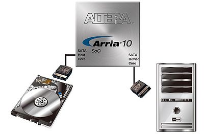
- Figure 4-4 PC and storage device connection to the Arria 10 SoC FPGA
- Figure 4-4 PC and storage device connection to the Arria 10 SoC FPGA

The transmitter and receiver signals of the SATA ports are connected directly to the Arria 10 SoC transceiver channels to provide SATA IO connectivity to both host and target devices. To verify the functionality of the SATA host/device ports, a connection can be established between the two ports by using a SATA cable as Figure 4-5 depicts the associated signals connected.Table 4-7 lists the SATA pin assignments, signal names and functions.
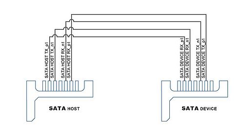
- Figure 4-5 Pin connection between SATA connectors
- Figure 4-5 Pin connection between SATA connectors
- Table 4-7 SATA Pin Assignments,Signal Names and Functions

Signal Name FPGA Pin Number Description I/O Standard Device SATA_DEVICE_REFCLK_p PIN_M31 SATA Device reference clock LVDS SATA_DEVICE_REFCLK_n PIN_M30 SATA Device reference clock LVDS SATA_DEVICE_RX_n0 PIN_D34 Differential receive data input after DC blocking capacitor HSSI DIFFERENTIAL I/O SATA_DEVICE_RX_n1 PIN_B34 Differential receive data input after DC blocking capacitor HSSI DIFFERENTIAL I/O SATA_DEVICE_TX_n0 PIN_B38 Differential transmit data output before DC blocking capacitor HSSI DIFFERENTIAL I/O SATA_DEVICE_TX_n1 PIN_A36 Differential transmit data output before DC blocking capacitor HSSI DIFFERENTIAL I/O SATA_DEVICE_TX_p0 PIN_B39 Differential transmit data output before DC blocking capacitor HSSI DIFFERENTIAL I/O SATA_DEVICE_TX_p1 PIN_A37 Differential transmit data output before DC blocking capacitor HSSI DIFFERENTIAL I/O SATA_DEVICE_RX_p0 PIN_D35 Differential receive data input after DC blocking capacitor HSSI DIFFERENTIAL I/O SATA_DEVICE_RX_p1 PIN_B35 Differential receive data input after DC blocking capacitor HSSI DIFFERENTIAL I/O Host SATA_HOST_REFCLK_p PIN_AF31 SATA Host reference clock LVDS SATA_HOST_REFCLK_n PIN_AF30 SATA Host reference clock LVDS SATA_HOST_TX_p0 PIN_AJ37 Differential transmit data output before DC blocking capacitor HSSI DIFFERENTIAL I/O SATA_HOST_TX_p1 PIN_AH39 Differential transmit data output before DC blocking capacitor HSSI DIFFERENTIAL I/O SATA_HOST_RX_p0 PIN_AE33 Differential receive data input after DC blocking capacitor HSSI DIFFERENTIAL I/O SATA_HOST_RX_p1 PIN_AF35 Differential receive data input after DC blocking capacitor HSSI DIFFERENTIAL I/O SATA_HOST_TX_n0 PIN_AJ36 Differential transmit data output before DC blocking capacitor HSSI DIFFERENTIAL I/O SATA_HOST_TX_n1 PIN_AH38 Differential transmit data output before DC blocking capacitor HSSI DIFFERENTIAL I/O SATA_HOST_RX_n0 PIN_AE32 Differential receive data input after DC blocking capacitor HSSI DIFFERENTIAL I/O SATA_HOST_RX_n1 PIN_AF34 Differential receive data input after DC blocking capacitor HSSI DIFFERENTIAL I/O
4.5 PCIe
The DE10-Advanced development board features one PCIe Express downstream interfaces (x4 lane) which are designed to interface with a PC motherboard x4 slot via PCIe cable and PCIe adapter card. Utilizing built-in transceivers on a Arria 10 SoC device, it is able to provide a fully integrated PCI Express compliant solution for multi-lane (x4) applications. With the PCI Express hard IP block incorporated in the Arria 10 SoC device, it will allow users to implement simple and fast protocols, as well as saving logic resources for logic applications.
The PCI Express interface supports complete PCI Express Gen1 at 2.5Gbps/lane, Gen2 at 5.0Gbps/lane, and Gen3 at 8.0Gbps/lane protocol stack solution compliant to PCI Express base specification 3.0 that includes PHY-MAC, Data Link, and transaction layer circuitry embedded in PCI Express hard IP blocks.
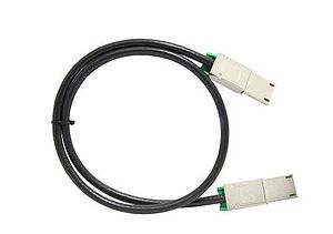
To use PCIe interface, two external associated devices will be needed to establish a link with PC. First, a PCIe half-height add-in host card with a PCIe x4 cable connector called PCA (PCIe Cabling Adapter Card and see Figure 4-5, it will be used to plug into the PCIe slot on a mother board.
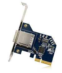
- Figure 4-5 PCIe Cabling Adaptor(PCA) card

Then,a PCIe x4 cable(See Figure 4-6) will be used to connect DE10-Advanced board and PCIe add-in card, the longest length is up to 3 meters.These two associated devices are not included in DE10-Advanced board. To purchase the PCA card as well as the external cable, please refer to Terasic website PCIe x4 Cable Adapterand PCIe x4 Gen.2 Cable.Table 4-8 summarizes the PCI Express pin assignments of the signal names relative to the Arria 10 SoC FPGA.PCIe pin connection is showed in Figure 4-7.
- Figure 4-6 PCIe External Cable
- Figure 4-6 PCIe External Cable


- Figure 4-7 PCI Express Pin Connection
- Table 4-8 PCIe Pin Assignments,Signal Names and Functions
Signal Name FPGA Pin Number Description I/O Standard PCIE_REFCLK_p PIN_AH31 PCIe reference clock LVDS PCIE_TX_p[0] PIN_AR37 PCIe Transmitter data p0 HSSI DIFFERENTIAL I/O PCIE_TX_p[1] PIN_AP39 PCIe Transmitter data p1 HSSI DIFFERENTIAL I/O PCIE_TX_p[2] PIN_AN37 PCIe Transmitter data p2 HSSI DIFFERENTIAL I/O PCIE_TX_p[3] PIN_AM39 PCIe Transmitter data p3 HSSI DIFFERENTIAL I/O PCIE_RX_p[0] PIN_AL33 PCIe Receiver data p0 HSSI DIFFERENTIAL I/O PCIE_RX_p[1] PIN_AM35 PCIe Receiver data p1 HSSI DIFFERENTIAL I/O PCIE_RX_p[2] PIN_AJ33 PCIe Receiver data p2 HSSI DIFFERENTIAL I/O PCIE_RX_p[3] PIN_AK35 PCIe Receiver data p3 HSSI DIFFERENTIAL I/O PCIE_PERST_n PIN_AW20 PCIe present,active low 1.8 V PCIE_WAKE_n PIN_AL19 PCIe wake 1.8 V
4.6 DDR4
The board supports 1GB of DDR4 SDRAM comprising of two x32bit DDR4 devices on FPGA side. The DDR4 signals are connected to the vertical I/O banks on the bottom edge of the FPGA. The DDR4 devices shipped with this board are running at 1067 MHz, for a total theoretical bandwidth of over 66Gbps. Figure 4-8 shows the connections between the DDR4 and Arria 10 SoC FPGA. Table 4-9 lists the pin assignments of DDR4 and its description with I/O standard.

- Figure 4-8 The connection between DDR4 and Arria 10 SoC FPGA
- Table 4-9 The pin assignments of DDR4 component and its description with I/O standard
FPGA Pin Number Signal Name Description I/O Standard PIN_AU7 DDR4B_REFCLK_p DDR4 A port Reference Clock p LVDS PIN_AJ11 DDR4B_A[0] Address [0] SSTL-12 PIN_AH12 DDR4B_A[1] Address [1] SSTL-12 PIN_AP11 DDR4B_A[2] Address [2] SSTL-12 PIN_AN11 DDR4B_A[3] Address [3] SSTL-12 PIN_AM10 DDR4B_A[4] Address [4] SSTL-12 PIN_AM11 DDR4B_A[5] Address [5] SSTL-12 PIN_AP9 DDR4B_A[6] Address [6] SSTL-12 PIN_AN9 DDR4B_A[7] Address [7] SSTL-12 PIN_AR10 DDR4B_A[8] Address [8] SSTL-12 PIN_AP10 DDR4B_A[9] Address [9] SSTL-12 PIN_AM9 DDR4B_A[10] Address [10] SSTL-12 PIN_AL10 DDR4B_A[11] Address [11] SSTL-12 PIN_AV8 DDR4B_A[12] Address [12] SSTL-12 PIN_AT8 DDR4B_A[13] Address [13] SSTL-12 PIN_AT9 DDR4B_A[14] Address [14]/WE_n SSTL-12 PIN_AR7 DDR4B_A[15] Address [15]/CAS_n SSTL-12 PIN_AR8 DDR4B_A[16] Address [16]/RAS_n SSTL-12 PIN_AU6 DDR4B_BA[0] Bank Select [0] SSTL-12 PIN_AP8 DDR4B_BA[1] Bank Select [1] SSTL-12 PIN_AN8 DDR4B_BG[0] Bank Group Select[0] SSTL-12 PIN_AJ14 DDR4B_BG[1] Bank Group Select[1] SSTL-12 PIN_AL13 DDR4B_CK Clock p0 DIFFERENTIAL 1.2-V SSTL PIN_AK13 DDR4B_CK_n Clock n0 DIFFERENTIAL 1.2-V SSTL PIN_AK10 DDR4B_CKE Clock Enable pin SSTL-12 PIN_AE12 DDR4B_DQS[0] Data Strobe p[0] DIFFERENTIAL 1.2-V POD PIN_AL7 DDR4B_DQS[1] Data Strobe p[1] DIFFERENTIAL 1.2-V POD PIN_AR6 DDR4B_DQS[2] Data Strobe p[2] DIFFERENTIAL 1.2-V POD PIN_AT2 DDR4B_DQS[3] Data Strobe p[3] DIFFERENTIAL 1.2-V POD PIN_AF13 DDR4B_DQS_n[0] Data Strobe n[0] DIFFERENTIAL 1.2-V POD PIN_AK8 DDR4B_DQS_n[1] Data Strobe n[1] DIFFERENTIAL 1.2-V POD PIN_AP6 DDR4B_DQS_n[2] Data Strobe n[2] DIFFERENTIAL 1.2-V POD PIN_AT3 DDR4B_DQS_n[3] Data Strobe n[3] DIFFERENTIAL 1.2-V POD PIN_AJ9 DDR4B_DQ[0] Data [0] 1.2-V POD PIN_AG11 DDR4B_DQ[1] Data [1] 1.2-V POD PIN_AF9 DDR4B_DQ[2] Data [2] 1.2-V POD PIN_AG12 DDR4B_DQ[3] Data [3] 1.2-V POD PIN_AG9 DDR4B_DQ[4] Data [4] 1.2-V POD PIN_AF12 DDR4B_DQ[5] Data [5] 1.2-V POD PIN_AJ10 DDR4B_DQ[6] Data [6] 1.2-V POD PIN_AG10 DDR4B_DQ[7] Data [7] 1.2-V POD PIN_AL9 DDR4B_DQ[8] Data [8] 1.2-V POD PIN_AH9 DDR4B_DQ[9] Data [9] 1.2-V POD PIN_AK6 DDR4B_DQ[10] Data [10] 1.2-V POD PIN_AK7 DDR4B_DQ[11] Data [11] 1.2-V POD PIN_AH8 DDR4B_DQ[12] Data [12] 1.2-V POD PIN_AH7 DDR4B_DQ[13] Data [13] 1.2-V POD PIN_AJ8 DDR4B_DQ[14] Data [14] 1.2-V POD PIN_AE11 DDR4B_DQ[15] Data [15] 1.2-V POD PIN_AT4 DDR4B_DQ[16] Data [16] 1.2-V POD PIN_AM7 DDR4B_DQ[17] Data [17] 1.2-V POD PIN_AP5 DDR4B_DQ[18] Data [18] 1.2-V POD PIN_AL5 DDR4B_DQ[19] Data [19] 1.2-V POD PIN_AM5 DDR4B_DQ[20] Data [20] 1.2-V POD PIN_AM6 DDR4B_DQ[21] Data [21] 1.2-V POD PIN_AM4 DDR4B_DQ[22] Data [22] 1.2-V POD PIN_AR5 DDR4B_DQ[23] Data [23] 1.2-V POD PIN_AP1 DDR4B_DQ[24] Data [24] 1.2-V POD PIN_AR3 DDR4B_DQ[25] Data [25] 1.2-V POD PIN_AN3 DDR4B_DQ[26] Data [26] 1.2-V POD PIN_AR1 DDR4B_DQ[27] Data [27] 1.2-V POD PIN_AU2 DDR4B_DQ[28] Data [28] 1.2-V POD PIN_AP4 DDR4B_DQ[29] Data [29] 1.2-V POD PIN_AR2 DDR4B_DQ[30] Data [30] 1.2-V POD PIN_AU1 DDR4B_DQ[31] Data [31] 1.2-V POD PIN_AF10 DDR4B_DM[0] DDR3 Data Mask[0] 1.2-V POD PIN_AL8 DDR4B_DM[1] DDR3 Data Mask[1] 1.2-V POD PIN_AN7 DDR4B_DM[2] DDR3 Data Mask[2] 1.2-V POD PIN_AN4 DDR4B_DM[3] DDR3 Data Mask[3] 1.2-V POD PIN_AJ13 DDR4B_CS_n[0] Chip Select SSTL-12 PIN_AH14 DDR4B_RESET_n Chip Reset 1.2 V PIN_AL12 DDR4A_ODT[0] On Die Termination SSTL-12 PIN_AM12 DDR4A_PAR Command and Address Parity Input SSTL-12 PIN_AH11 DDR4A_ALERT_n Register ALERT_n output SSTL-12 PIN_AH13 DDR4A_ACT_n Activation Command Input SSTL-12 PIN_AW8 DDR4A_RZQ External reference ball for output drive calibration 1.2 V
The development board also supports one bank of DDR4 SDRAM SO-DIMM on FPGA side. It is wired to support a maximum capacity of 8GB with a 72-bit data bus. Using differential DQS signaling for the DDR4 SDRAM interfaces, it is capable of running at up to 1067MHz memory clock for a maximum theoretical bandwidth up to 132Gbps. Figure 4-9 shows the connections between the DDR4 SDRAM SODIMM and Arria 10 SoC FPGA. The pin assignments for DDR4 SDRAM SO-DIMM are listed in Table 4-10.

Figure 4-9 The connection between the DDR4 SDRAM SO-DIMM and Arria 10 SoC FPGA
- Table 4-10 The pin assignments for DDR4 SDRAM SO-DIMM
FPGA Pin Number Signal Name Description I/O Standard PIN_AB12 DDR4A_REFCLK_p DDR4 A port Reference Clock p LVDS PIN_AC1 DDR4A_A[0] Address [0] SSTL-12 PIN_AB1 DDR4A_A[1] Address [1] SSTL-12 PIN_AB4 DDR4A_A[2] Address [2] SSTL-12 PIN_AA5 DDR4A_A[3] Address [3] SSTL-12 PIN_AA3 DDR4A_A[4] Address [4] SSTL-12 PIN_AA4 DDR4A_A[5] Address [5] SSTL-12 PIN_Y2 DDR4A_A[6] Address [6] SSTL-12 PIN_AA2 DDR4A_A[7] Address [7] SSTL-12 PIN_AB5 DDR4A_A[8] Address [8] SSTL-12 PIN_AB6 DDR4A_A[9] Address [9] SSTL-12 PIN_W5 DDR4A_A[10] Address [10] SSTL-12 PIN_Y5 DDR4A_A[11] Address [11] SSTL-12 PIN_AA9 DDR4A_A[12] Address [12] SSTL-12 PIN_AB7 DDR4A_A[13] Address [13] SSTL-12 PIN_AA7 DDR4A_A[14] Address [14]/WE_n SSTL-12 PIN_AB10 DDR4A_A[15] Address [15]/CAS_n SSTL-12 PIN_AB11 DDR4A_A[16] Address [16]/RAS_n SSTL-12 PIN_Y7 DDR4A_BA[0] Bank Select [0] SSTL-12 PIN_AB9 DDR4A_BA[1] Bank Select [1] SSTL-12 PIN_AA10 DDR4A_BG[0] Bank Group Select[0] SSTL-12 PIN_AE2 DDR4A_BG[1] Bank Group Select[1] SSTL-12 PIN_AD3 DDR4A_CK Clock p0 DIFFERENTIAL 1.2-V SSTL PIN_AD4 DDR4A_CK_n Clock n0 DIFFERENTIAL 1.2-V SSTL PIN_AC2 DDR4A_CKE Clock Enable pin SSTL-12 PIN_AE8 DDR4A_DQS[0] Data Strobe p[0] DIFFERENTIAL 1.2-V POD PIN_AF7 DDR4A_DQS[1] Data Strobe p[1] DIFFERENTIAL 1.2-V POD PIN_AN1 DDR4A_DQS[2] Data Strobe p[2] DIFFERENTIAL 1.2-V POD PIN_AH2 DDR4A_DQS[3] Data Strobe p[3] DIFFERENTIAL 1.2-V POD PIN_P1 DDR4A_DQS[4] Data Strobe p[4] DIFFERENTIAL 1.2-V POD PIN_J3 DDR4A_DQS[5] Data Strobe p[5] DIFFERENTIAL 1.2-V POD PIN_R5 DDR4A_DQS[6] Data Strobe p[6] DIFFERENTIAL 1.2-V POD PIN_V9 DDR4A_DQS[7] Data Strobe p[7] DIFFERENTIAL 1.2-V POD PIN_V2 DDR4A_DQS[8] Data Strobe p[8] DIFFERENTIAL 1.2-V POD PIN_AD8 DDR4A_DQS_n[0] Data Strobe n[0] DIFFERENTIAL 1.2-V POD PIN_AE7 DDR4A_DQS_n[1] Data Strobe n[1] DIFFERENTIAL 1.2-V POD PIN_AN2 DDR4A_DQS_n[2] Data Strobe n[2] DIFFERENTIAL 1.2-V POD PIN_AH3 DDR4A_DQS_n[3] Data Strobe n[3] DIFFERENTIAL 1.2-V POD PIN_R1 DDR4A_DQS_n[4] Data Strobe n[4] DIFFERENTIAL 1.2-V POD PIN_K3 DDR4A_DQS_n[5] Data Strobe n[5] DIFFERENTIAL 1.2-V POD PIN_R6 DDR4A_DQS_n[6] Data Strobe n[6] DIFFERENTIAL 1.2-V POD PIN_W9 DDR4A_DQS_n[7] Data Strobe n[7] DIFFERENTIAL 1.2-V POD PIN_V3 DDR4A_DQS_n[8] Data Strobe n[8] DIFFERENTIAL 1.2-V POD PIN_AC11 DDR4A_DQ[0] Data [0] 1.2-V POD PIN_AD10 DDR4A_DQ[1] Data [1] 1.2-V POD PIN_AC9 DDR4A_DQ[2] Data [2] 1.2-V POD PIN_AG7 DDR4A_DQ[3] Data [3] 1.2-V POD PIN_AD13 DDR4A_DQ[4] Data [4] 1.2-V POD PIN_AD11 DDR4A_DQ[5] Data [5] 1.2-V POD PIN_AC8 DDR4A_DQ[6] Data [6] 1.2-V POD PIN_AF8 DDR4A_DQ[7] Data [7] 1.2-V POD PIN_AE6 DDR4A_DQ[8] Data [8] 1.2-V POD PIN_AJ6 DDR4A_DQ[9] Data [9] 1.2-V POD PIN_AG6 DDR4A_DQ[10] Data [10] 1.2-V POD PIN_AD6 DDR4A_DQ[11] Data [11] 1.2-V POD PIN_AG5 DDR4A_DQ[12] Data [12] 1.2-V POD PIN_AK5 DDR4A_DQ[13] Data [13] 1.2-V POD PIN_AC7 DDR4A_DQ[14] Data [14] 1.2-V POD PIN_AH6 DDR4A_DQ[15] Data [15] 1.2-V POD PIN_AK1 DDR4A_DQ[16] Data [16] 1.2-V POD PIN_AL4 DDR4A_DQ[17] Data [17] 1.2-V POD PIN_AJ4 DDR4A_DQ[18] Data [18] 1.2-V POD PIN_AM1 DDR4A_DQ[19] Data [19] 1.2-V POD PIN_AK3 DDR4A_DQ[20] Data [20] 1.2-V POD PIN_AL2 DDR4A_DQ[21] Data [21] 1.2-V POD PIN_AJ3 DDR4A_DQ[22] Data [22] 1.2-V POD PIN_AM2 DDR4A_DQ[23] Data [23] 1.2-V POD PIN_AF2 DDR4A_DQ[24] Data [24] 1.2-V POD PIN_AH1 DDR4A_DQ[25] Data [25] 1.2-V POD PIN_AG4 DDR4A_DQ[26] Data [26] 1.2-V POD PIN_AE5 DDR4A_DQ[27] Data [27] 1.2-V POD PIN_AF3 DDR4A_DQ[28] Data [28] 1.2-V POD PIN_AH4 DDR4A_DQ[29] Data [29] 1.2-V POD PIN_AG1 DDR4A_DQ[30] Data [30] 1.2-V POD PIN_AF4 DDR4A_DQ[31] Data [31] 1.2-V POD PIN_K1 DDR4A_DQ[32] Data [32] 1.2-V POD PIN_P4 DDR4A_DQ[33] Data [33] 1.2-V POD PIN_N2 DDR4A_DQ[34] Data [34] 1.2-V POD PIN_K2 DDR4A_DQ[35] Data [35] 1.2-V POD PIN_M2 DDR4A_DQ[36] Data [36] 1.2-V POD PIN_P3 DDR4A_DQ[37] Data [37] 1.2-V POD PIN_N1 DDR4A_DQ[38] Data [38] 1.2-V POD PIN_J1 DDR4A_DQ[39] Data [39] 1.2-V POD PIN_N3 DDR4A_DQ[40] Data [40] 1.2-V POD PIN_P5 DDR4A_DQ[41] Data [41] 1.2-V POD PIN_M5 DDR4A_DQ[42] Data [42] 1.2-V POD PIN_R2 DDR4A_DQ[43] Data [43] 1.2-V POD PIN_N4 DDR4A_DQ[44] Data [44] 1.2-V POD PIN_P6 DDR4A_DQ[45] Data [45] 1.2-V POD PIN_L4 DDR4A_DQ[46] Data [46] 1.2-V POD PIN_R3 DDR4A_DQ[47] Data [47] 1.2-V POD PIN_V6 DDR4A_DQ[48] Data [48] 1.2-V POD PIN_T7 DDR4A_DQ[49] Data [49] 1.2-V POD PIN_U5 DDR4A_DQ[50] Data [50] 1.2-V POD PIN_U7 DDR4A_DQ[51] Data [51] 1.2-V POD PIN_T4 DDR4A_DQ[52] Data [52] 1.2-V POD PIN_W6 DDR4A_DQ[53] Data [53] 1.2-V POD PIN_T3 DDR4A_DQ[54] Data [54] 1.2-V POD PIN_U6 DDR4A_DQ[55] Data [55] 1.2-V POD PIN_W8 DDR4A_DQ[56] Data [56] 1.2-V POD PIN_Y12 DDR4A_DQ[57] Data [57] 1.2-V POD PIN_Y11 DDR4A_DQ[58] Data [58] 1.2-V POD PIN_W10 DDR4A_DQ[59] Data [59] 1.2-V POD PIN_Y13 DDR4A_DQ[60] Data [60] 1.2-V POD PIN_Y8 DDR4A_DQ[61] Data [61] 1.2-V POD PIN_Y10 DDR4A_DQ[62] Data [62] 1.2-V POD PIN_W11 DDR4A_DQ[63] Data [63] 1.2-V POD PIN_V1 DDR4A_DQ[64] Data [64] 1.2-V POD PIN_Y1 DDR4A_DQ[65] Data [65] 1.2-V POD PIN_W3 DDR4A_DQ[66] Data [66] 1.2-V POD PIN_W1 DDR4A_DQ[67] Data [67] 1.2-V POD PIN_Y3 DDR4A_DQ[68] Data [68] 1.2-V POD PIN_W4 DDR4A_DQ[69] Data [69] 1.2-V POD PIN_U1 DDR4A_DQ[70] Data [70] 1.2-V POD PIN_U2 DDR4A_DQ[71] Data [71] 1.2-V POD PIN_AD9 DDR4A_DBI_n[0] Data Bus Inversion [0] 1.2-V POD PIN_AJ5 DDR4A_DBI_n[1] Data Bus Inversion [1] 1.2-V POD PIN_AK2 DDR4A_DBI_n[2] Data Bus Inversion [2] 1.2-V POD PIN_AG2 DDR4A_DBI_n[3] Data Bus Inversion [3] 1.2-V POD PIN_L2 DDR4A_DBI_n[4] Data Bus Inversion [4] 1.2-V POD PIN_L3 DDR4A_DBI_n[5] Data Bus Inversion [5] 1.2-V POD PIN_U4 DDR4A_DBI_n[6] Data Bus Inversion [6] 1.2-V POD PIN_V8 DDR4A_DBI_n[7] Data Bus Inversion [7] 1.2-V POD PIN_V4 DDR4A_DBI_n[8] Data Bus Inversion [8] 1.2-V POD PIN_AE1 DDR4A_CS_n Chip Select SSTL-12 PIN_AE3 DDR4A_RESET_n Chip Reset 1.2 V PIN_AC3 DDR4A_ODT On Die Termination SSTL-12 PIN_AC6 DDR4A_PAR Command and Address Parity Input SSTL-12 PIN_AC12 DDR4A_ALERT_n Register ALERT_n output SSTL-12 PIN_AD1 DDR4A_ACT_n Activation Command Input SSTL-12 PIN_T5 DDR4A_EVENT_n Chip Temperature Event 1.2 V PIN_AD5 DDR4A_AC_R[0] Reserved for QDRII+/RLDRAM3 SSTL-12 PIN_Y6 DDR4A_AC_R[1] Reserved for QDRII+/RLDRAM3 SSTL-12 PIN_AC4 DDR4A_C[0] Reserved for QDRII+/RLDRAM3 SSTL-12 PIN_AB2 DDR4A_C[1] Reserved for QDRII+/RLDRAM3 SSTL-12 PIN_AA8 DDR4A_RZQ External reference ball for output drive calibration 1.2 V
The DDR4 SDRAM SO-DIMM socket can support many kinds of memory devices, such as standard DDR4 SO-DIMM with ECC up to 8GB at 1067MHz, Terasic QDRII+ module with DDR4 SO-DIMM interface, Terasic RLDRAM3 module with DDR4 SO-DIMM interface, as shown in Figure 4-10, Figure 4-11 and Figure 4-12.


Figure 4-10 Standard DDR4 SO-DIMM with ECC Figure 4-11 Terasic QDRII+ module with DDR4 SO-DIMM interface

Figure 4-12 Terasic RLDRAM3 module with DDR4 SO-DIMM interface
4.7 HDMI Transmitter and Receiver
The DE10-Advanced board features HDMI transmitter and receiver.
For HDMI transmitter,as shown in Figure 4-13. The board features a Transition Minimized Differential Signal(TMDS) retimer IC (TI:SN75DP159). Users can implement Intel or third-party IP in FPGA, HDMI image or video datas is encoded to TMDS signal and output from FPGA transceiver. The signals transmit to the retimer IC and display on HDMI monitor through HDMI connector.
For HDMI Receiver, it features a Redriver IC(DIDOES:PI3HDX1204B1). It transmits the input TMDS signal into FPGA, and decoded to image video datas by Intel or third-party IP, then will be processed next step.
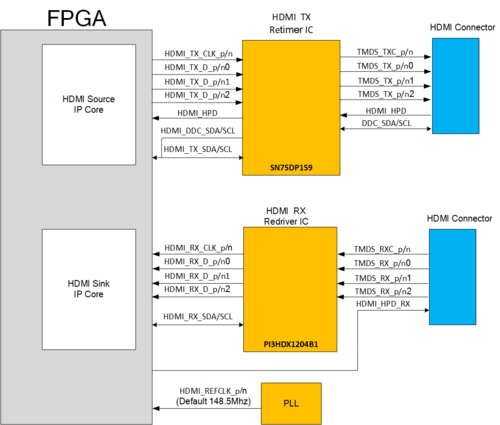
- Figure 4-13 The HDMI transceiver interface of the DE10-Advanced
- Table 4-11 HDMI TX and RX port Pin Assignments, Signal Names and Functions

Signal Name FPGA Pin Number Description I/O Standard HDMI_TX_CLK_p V39 TX TMDS clock channel HSSI Differential I/O HDMI_TX_D_p[0] U37 TX TMDS data channel 0 HSSI Differential I/O HDMI_TX_D_p[1] T39 TX TMDS data channel 1 HSSI Differential I/O HDMI_TX_D_p[2] R37 TX TMDS data channel 2 HSSI Differential I/O HDMI_TX_SCL A28 I2C clock of the TX retimer IC and DCC 1.8V HDMI_TX_SDA A27 I2C data of the TX retimer IC and DCC 1.8V HDMI_HPD AF28 TX Hot Plug Detect 1.8V HDMI_RX_CLK_p Y31 RX TMDS clock channel HSSI Differential I/O HDMI_RX_D_p[0] Y35 RX TMDS data channel 0 HSSI Differential I/O HDMI_RX_D_p[1] W37 RX TMDS data channel 1 HSSI Differential I/O HDMI_RX_D_p[2] W33 RX TMDS data channel 2 HSSI Differential I/O HDMI_RX_SCL V7 I2C clock of the RX redriver IC 1.2 V HDMI_RX_SDA T2 I2C clock of the RX redriver IC 1.2 V HDMI_HPD_RX AG27 RX Hot Plug Detect 1.8V HDMI_RX_5V_N C29 Detect if the TX terminal has 5V output 1.8V HDMI_REFCLK_p V31 HDMI Reference clock from on board PLL LVDS
4.8 Gigabit Ethernet
The development board supports one RJ45 10/100/1000 base-T Ethernet using Marvell 88E1111. SGMII AC coupling interface is used between PHY and FPGA transceiver.The device is an auto-negotiating Ethernet PHY with an SGMII interface to the FPGA. The Arria 10 SoC FPGA can communicate with the LVDS interfaces at up to 1.6 Gbps, which is faster than 1.25 Gbps for SGMII. The MAC function must be provided in the FPGA for typical networking applications. The Marvell 88E1111 PHY uses 2.5-V and 1.1-V power rails and requires a 25MHz reference clock driven from a dedicated oscillator. It interfaces to an RJ-45 with internal magnetics for driving copper lines with Ethernet traffic.Figure 4-2 shows the SGMII interface between the FPGA and Marvell 88E1111 PHY. Table 4-2 lists the Ethernet PHY interface pin assignments.
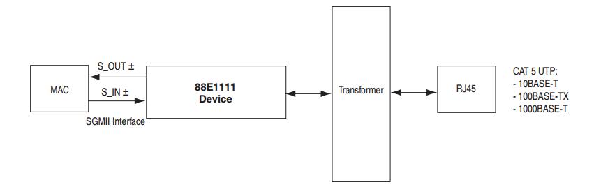
- Figure 4-2 SGMII Interface between FPGA and Marvell 88E1111 PHY

- Table 4-2 Ethernet PHY Pin Assignments, Signal Names and Functions
Signal Name FPGA Pin Number Description I/O Standard ETH_TX_p PIN_AP19 SGMII TX data LVDS ETH_RX_p PIN_AM20 SGMII RX data LVDS ETH_INT_n PIN_AU19 Management bus interrupt 1.8V ETH_MDC PIN_AT19 Management bus control 1.8V ETH_MDIO PIN_AJ20 Management bus data 1.8V ETH_RST_n PIN_AK20 Device reset 1.8V
4.9 FMC Connector
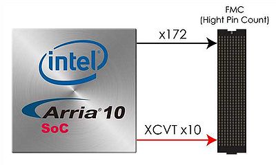
The FPGA Mezzanine Card (FMC) interface provides a mechanism to extend the peripheral-set of an FPGA host board by means of add-on daughter cards, which can address today’s high speed signaling requirements as well as low-speed device interface support.The FMC interfaces support JTAG,clock outputs and inputs,high-speed serial I/O (transceivers),and single-ended or differential signaling.
There is one FMC connector on the DE10-Advanced board,it is a High Pin Count (HPC) size of connector,The HPC connector on DE10-Advanced board can provides 172 user-define,single-ended signals (include clock signals) and 10 serial transceiver pairs.Figure 4-10 is the FMC connector on DE10-Advanced board
- Figure 4-10 FMC connector on DE10-Advanced board
- Table 4-11 FMC Connector Pin Assignments, Signal Names and Functions
- Figure 4-10 FMC connector on DE10-Advanced board

Signal Name FPGA Pin Number Description I/O Standard FMC_CLK2_BIDIR_p PIN_AW18 FMC bidirection Clock signal 1.8 V FMC_CLK2_BIDIR_n PIN_AV17 FMC bidirection Clock signal 1.8 V FMC_CLK3_BIDIR_p PIN_C1 FMC bidirection Clock signal 1.8 V FMC_CLK3_BIDIR_n PIN_D1 FMC bidirection Clock signal 1.8 V FMC_CLK_M2C_p[0] PIN_K5 Clock input 0 1.8 V FMC_CLK_M2C_p[1] PIN_AW14 Clock input 1 1.8 V FMC_CLK_M2C_n[0] PIN_L5 Clock input 0 1.8 V FMC_CLK_M2C_n[1] PIN_AW15 Clock input 1 1.8 V FMC_HA_p[0] PIN_K12 FMC data bus 1.8 V FMC_HA_p[1] PIN_M12 FMC data bus 1.8 V FMC_HA_p[2] PIN_D10 FMC data bus 1.8 V FMC_HA_p[3] PIN_E12 FMC data bus 1.8 V FMC_HA_p[4] PIN_H13 FMC data bus 1.8 V FMC_HA_p[5] PIN_J11 FMC data bus 1.8 V FMC_HA_p[6] PIN_N13 FMC data bus 1.8 V FMC_HA_p[7] PIN_L13 FMC data bus 1.8 V FMC_HA_p[8] PIN_J14 FMC data bus 1.8 V FMC_HA_p[9] PIN_F13 FMC data bus 1.8 V FMC_HA_p[10] PIN_D13 FMC data bus 1.8 V FMC_HA_p[11] PIN_G14 FMC data bus 1.8 V FMC_HA_p[12] PIN_A10 FMC data bus 1.8 V FMC_HA_p[13] PIN_G12 FMC data bus 1.8 V FMC_HA_p[14] PIN_A12 FMC data bus 1.8 V FMC_HA_p[15] PIN_A7 FMC data bus 1.8 V FMC_HA_p[16] PIN_A9 FMC data bus 1.8 V FMC_HA_p[17] PIN_C12 FMC data bus 1.8 V FMC_HA_p[18] PIN_B11 FMC data bus 1.8 V FMC_HA_p[19] PIN_M7 FMC data bus 1.8 V FMC_HA_p[20] PIN_F10 FMC data bus 1.8 V FMC_HA_p[21] PIN_C9 FMC data bus 1.8 V FMC_HA_p[22] PIN_C8 FMC data bus 1.8 V FMC_HA_p[23] PIN_G11 FMC data bus 1.8 V FMC_HA_n[0] PIN_L12 FMC data bus 1.8 V FMC_HA_n[1] PIN_N12 FMC data bus 1.8 V FMC_HA_n[2] PIN_E10 FMC data bus 1.8 V FMC_HA_n[3] PIN_F12 FMC data bus 1.8 V FMC_HA_n[4] PIN_J13 FMC data bus 1.8 V FMC_HA_n[5] PIN_K11 FMC data bus 1.8 V FMC_HA_n[6] PIN_P13 FMC data bus 1.8 V FMC_HA_n[7] PIN_L14 FMC data bus 1.8 V FMC_HA_n[8] PIN_K13 FMC data bus 1.8 V FMC_HA_n[9] PIN_F14 FMC data bus 1.8 V FMC_HA_n[10] PIN_E13 FMC data bus 1.8 V FMC_HA_n[11] PIN_H14 FMC data bus 1.8 V FMC_HA_n[12] PIN_B10 FMC data bus 1.8 V FMC_HA_n[13] PIN_H12 FMC data bus 1.8 V FMC_HA_n[14] PIN_B12 FMC data bus 1.8 V FMC_HA_n[15] PIN_A8 FMC data bus 1.8 V FMC_HA_n[16] PIN_B9 FMC data bus 1.8 V FMC_HA_n[17] PIN_C13 FMC data bus 1.8 V FMC_HA_n[18] PIN_C11 FMC data bus 1.8 V FMC_HA_n[19] PIN_N7 FMC data bus 1.8 V FMC_HA_n[20] PIN_G10 FMC data bus 1.8 V FMC_HA_n[21] PIN_D9 FMC data bus 1.8 V FMC_HA_n[22] PIN_D8 FMC data bus 1.8 V FMC_HA_n[23] PIN_H11 FMC data bus 1.8 V FMC_HB_p[0] PIN_E1 FMC data bus 1.8 V FMC_HB_p[1] PIN_G4 FMC data bus 1.8 V FMC_HB_p[2] PIN_N8 FMC data bus 1.8 V FMC_HB_p[3] PIN_J4 FMC data bus 1.8 V FMC_HB_p[4] PIN_H2 FMC data bus 1.8 V FMC_HB_p[5] PIN_G5 FMC data bus 1.8 V FMC_HB_p[6] PIN_D3 FMC data bus 1.8 V FMC_HB_p[7] PIN_A2 FMC data bus 1.8 V FMC_HB_p[8] PIN_B1 FMC data bus 1.8 V FMC_HB_p[9] PIN_AT13 FMC data bus 1.8 V FMC_HB_p[10] PIN_AM17 FMC data bus 1.8 V FMC_HB_p[11] PIN_AJ16 FMC data bus 1.8 V FMC_HB_p[12] PIN_AW13 FMC data bus 1.8 V FMC_HB_p[13] PIN_AV14 FMC data bus 1.8 V FMC_HB_p[14] PIN_AP14 FMC data bus 1.8 V FMC_HB_p[15] PIN_AK16 FMC data bus 1.8 V FMC_HB_p[16] PIN_AU16 FMC data bus 1.8 V FMC_HB_p[17] PIN_AT17 FMC data bus 1.8 V FMC_HB_p[18] PIN_AM15 FMC data bus 1.8 V FMC_HB_p[19] PIN_AR15 FMC data bus 1.8 V FMC_HB_p[20] PIN_AP16 FMC data bus 1.8 V FMC_HB_p[21] PIN_AV18 FMC data bus 1.8 V FMC_HB_n[0] PIN_E2 FMC data bus 1.8 V FMC_HB_n[1] PIN_H4 FMC data bus 1.8 V FMC_HB_n[2] PIN_P8 FMC data bus 1.8 V FMC_HB_n[3] PIN_J5 FMC data bus 1.8 V FMC_HB_n[4] PIN_H3 FMC data bus 1.8 V FMC_HB_n[5] PIN_H6 FMC data bus 1.8 V FMC_HB_n[6] PIN_E3 FMC data bus 1.8 V FMC_HB_n[7] PIN_B2 FMC data bus 1.8 V FMC_HB_n[8] PIN_C2 FMC data bus 1.8 V FMC_HB_n[9] PIN_AT14 FMC data bus 1.8 V FMC_HB_n[10] PIN_AL17 FMC data bus 1.8 V FMC_HB_n[11] PIN_AH16 FMC data bus 1.8 V FMC_HB_n[12] PIN_AV13 FMC data bus 1.8 V FMC_HB_n[13] PIN_AU14 FMC data bus 1.8 V FMC_HB_n[14] PIN_AP15 FMC data bus 1.8 V FMC_HB_n[15] PIN_AK17 FMC data bus 1.8 V FMC_HB_n[16] PIN_AU17 FMC data bus 1.8 V FMC_HB_n[17] PIN_AT18 FMC data bus 1.8 V FMC_HB_n[18] PIN_AM16 FMC data bus 1.8 V FMC_HB_n[19] PIN_AR16 FMC data bus 1.8 V FMC_HB_n[20] PIN_AN16 FMC data bus 1.8 V FMC_HB_n[21] PIN_AV19 FMC data bus 1.8 V FMC_LA_p[0] PIN_A3 FMC data bus 1.8 V FMC_LA_p[1] PIN_B4 FMC data bus 1.8 V FMC_LA_p[2] PIN_T9 FMC data bus 1.8 V FMC_LA_p[3] PIN_M10 FMC data bus 1.8 V FMC_LA_p[4] PIN_U9 FMC data bus 1.8 V FMC_LA_p[5] PIN_J10 FMC data bus 1.8 V FMC_LA_p[6] PIN_H8 FMC data bus 1.8 V FMC_LA_p[7] PIN_L9 FMC data bus 1.8 V FMC_LA_p[8] PIN_M9 FMC data bus 1.8 V FMC_LA_p[9] PIN_G6 FMC data bus 1.8 V FMC_LA_p[10] PIN_E8 FMC data bus 1.8 V FMC_LA_p[11] PIN_B6 FMC data bus 1.8 V FMC_LA_p[12] PIN_A5 FMC data bus 1.8 V FMC_LA_p[13] PIN_D5 FMC data bus 1.8 V FMC_LA_p[14] PIN_B7 FMC data bus 1.8 V FMC_LA_p[15] PIN_E6 FMC data bus 1.8 V FMC_LA_p[16] PIN_E5 FMC data bus 1.8 V FMC_LA_p[17] PIN_F9 FMC data bus 1.8 V FMC_LA_p[18] PIN_K8 FMC data bus 1.8 V FMC_LA_p[19] PIN_R8 FMC data bus 1.8 V FMC_LA_p[20] PIN_F7 FMC data bus 1.8 V FMC_LA_p[21] PIN_C4 FMC data bus 1.8 V FMC_LA_p[22] PIN_U11 FMC data bus 1.8 V FMC_LA_p[23] PIN_V11 FMC data bus 1.8 V FMC_LA_p[24] PIN_R11 FMC data bus 1.8 V FMC_LA_p[25] PIN_F2 FMC data bus 1.8 V FMC_LA_p[26] PIN_R7 FMC data bus 1.8 V FMC_LA_p[27] PIN_T12 FMC data bus 1.8 V FMC_LA_p[28] PIN_J6 FMC data bus 1.8 V FMC_LA_p[29] PIN_G1 FMC data bus 1.8 V FMC_LA_p[30] PIN_K7 FMC data bus 1.8 V FMC_LA_p[31] PIN_P10 FMC data bus 1.8 V FMC_LA_p[32] PIN_M6 FMC data bus 1.8 V FMC_LA_p[33] PIN_N11 FMC data bus 1.8 V FMC_LA_n[0] PIN_A4 FMC data bus 1.8 V FMC_LA_n[1] PIN_C3 FMC data bus 1.8 V FMC_LA_n[2] PIN_T10 FMC data bus 1.8 V FMC_LA_n[3] PIN_M11 FMC data bus 1.8 V FMC_LA_n[4] PIN_U10 FMC data bus 1.8 V FMC_LA_n[5] PIN_K10 FMC data bus 1.8 V FMC_LA_n[6] PIN_J8 FMC data bus 1.8 V FMC_LA_n[7] PIN_L10 FMC data bus 1.8 V FMC_LA_n[8] PIN_N9 FMC data bus 1.8 V FMC_LA_n[9] PIN_H7 FMC data bus 1.8 V FMC_LA_n[10] PIN_F8 FMC data bus 1.8 V FMC_LA_n[11] PIN_C6 FMC data bus 1.8 V FMC_LA_n[12] PIN_B5 FMC data bus 1.8 V FMC_LA_n[13] PIN_D6 FMC data bus 1.8 V FMC_LA_n[14] PIN_C7 FMC data bus 1.8 V FMC_LA_n[15] PIN_E7 FMC data bus 1.8 V FMC_LA_n[16] PIN_F5 FMC data bus 1.8 V FMC_LA_n[17] PIN_G9 FMC data bus 1.8 V FMC_LA_n[18] PIN_L8 FMC data bus 1.8 V FMC_LA_n[19] PIN_P9 FMC data bus 1.8 V FMC_LA_n[20] PIN_G7 FMC data bus 1.8 V FMC_LA_n[21] PIN_D4 FMC data bus 1.8 V FMC_LA_n[22] PIN_U12 FMC data bus 1.8 V FMC_LA_n[23] PIN_V12 FMC data bus 1.8 V FMC_LA_n[24] PIN_R12 FMC data bus 1.8 V FMC_LA_n[25] PIN_G2 FMC data bus 1.8 V FMC_LA_n[26] PIN_T8 FMC data bus 1.8 V FMC_LA_n[27] PIN_T13 FMC data bus 1.8 V FMC_LA_n[28] PIN_K6 FMC data bus 1.8 V FMC_LA_n[29] PIN_H1 FMC data bus 1.8 V FMC_LA_n[30] PIN_L7 FMC data bus 1.8 V FMC_LA_n[31] PIN_R10 FMC data bus 1.8 V FMC_LA_n[32] PIN_N6 FMC data bus 1.8 V FMC_LA_n[33] PIN_P11 FMC data bus 1.8 V FMC_GBTCLK_M2C_p[0] PIN_P31 LVDS input from the installed FMC card to dedicated reference clock inputs LVDS FMC_GBTCLK_M2C_p[1] PIN_K31 LVDS input from the installed FMC card to dedicated reference clock inputs LVDS FMC_REFCLK_p PIN_T31 Reference Clock LVDS FMC_DP_C2M_p[0] PIN_M39 Transmit channel HSSI DIFFERENTIAL I/O FMC_DP_C2M_p[1] PIN_L37 Transmit channel HSSI DIFFERENTIAL I/O FMC_DP_C2M_p[2] PIN_K39 Transmit channel HSSI DIFFERENTIAL I/O FMC_DP_C2M_p[3] PIN_J37 Transmit channel HSSI DIFFERENTIAL I/O FMC_DP_C2M_p[4] PIN_H39 Transmit channel HSSI DIFFERENTIAL I/O FMC_DP_C2M_p[5] PIN_G37 Transmit channel HSSI DIFFERENTIAL I/O FMC_DP_C2M_p[6] PIN_F39 Transmit channel HSSI DIFFERENTIAL I/O FMC_DP_C2M_p[7] PIN_E37 Transmit channel HSSI DIFFERENTIAL I/O FMC_DP_C2M_p[8] PIN_D39 Transmit channel HSSI DIFFERENTIAL I/O FMC_DP_C2M_p[9] PIN_C37 Transmit channel HSSI DIFFERENTIAL I/O FMC_DP_M2C_p[0] PIN_P35 Transmit channel HSSI DIFFERENTIAL I/O FMC_DP_M2C_p[1] PIN_R33 Transmit channel HSSI DIFFERENTIAL I/O FMC_DP_M2C_p[2] PIN_M35 Transmit channel HSSI DIFFERENTIAL I/O FMC_DP_M2C_p[3] PIN_N33 Transmit channel HSSI DIFFERENTIAL I/O FMC_DP_M2C_p[4] PIN_K35 Transmit channel HSSI DIFFERENTIAL I/O FMC_DP_M2C_p[5] PIN_L33 Transmit channel HSSI DIFFERENTIAL I/O FMC_DP_M2C_p[6] PIN_H35 Transmit channel HSSI DIFFERENTIAL I/O FMC_DP_M2C_p[7] PIN_J33 Transmit channel HSSI DIFFERENTIAL I/O FMC_DP_M2C_p[8] PIN_F35 Transmit channel HSSI DIFFERENTIAL I/O FMC_DP_M2C_p[9] PIN_G33 Transmit channel HSSI DIFFERENTIAL I/O FMC_GA[0] PIN_E11 FMC geographical address 0 1.8 V FMC_GA[1] PIN_AL18 FMC geographical address 1 1.8 V FMC_SCL PIN_J9 Management serial clock line 1.8 V FMC_SDA PIN_F4 Management serial data line 1.8 V
4.10 Temperature Sensor,Fan Control and Power Monitor
The FPGA board is equipped with a temperature sensor, TMP441AIDCNT, which provides temperature sensing.This functions is accomplished by connecting the temperature sensor to the internal temperature sensing diode of the Arria 10 SoC device. The temperature status and alarm threshold registers of the temperature sensor can be programmed by a two-wire SMBus, which is connected to the Arria 10 SoC FPGA. In addition, the 7-bit POR slave address for this sensor is set to‘0011100b'.
A 3-pin +12V fan located on J22 of the FPGA board is intended to reduce the temperature of the FPGA.The board is equipped with a Fan-Speed regulator and monitor MAX6650 with an I2C/SMBus interfaces,Users regulate and monitor the speed of fan depending on the measured system temperature.
The DE10-Advanced has implemented a power monitor chip to monitor the board input power voltage and current.Figure 4-10 shows the connection between the power monitor chip and the Arria 10 SoC FPGA.The power monitor chip monitors both shunt voltage drops and board input power voltage allows user to monitor the total board power consumption. Programmable calibration value,conversion times,and averaging,combined with an internal multiplier,enable direct readouts of current in amperes and power in watts.Note that,the temperature sensor,fan control and power monitor share the same I2C/SMBUS.

Figure 4-10 Connections between the temperature sensor/fan control/power monitor and the Arria 10 SoC FPGA
- Table 4-12 Temperature Sensor and Fan Speed Control Pin Assignments,Schematic Signal Names and Functions
Schematic Signal Name Description I/O Standard Arria 10 SoC Pin Number TEMPDIODEp Positive pin of temperature diode in Arria 10 -- -- TEMPDIODEn Negative pin of temperature diode in Arria 10 -- -- FPGA_I2C_SCL SMBus clock 1.8V M1 FPGA_I2C_SDA SMBus data 1.8V M4 FAN_ALERT Active-low ALERT input 1.8V E25
4.11 Gyroscope, Accelerometer and Magnetometer
The DE10-Advanced board is equipped with a Motion-Tracking device named MPU-9250. The MPU-9250 is a 9-axis Motion-Tracking device that combines a 3-axis gyroscope, 3-axis accelerometer and 3-axis magnetometer. Detail features of these sensors are listed below.
4.11.1 Gyroscope
The MPU-9250 consists of three independent vibratory MEMS rate gyroscopes, which detect rotation about the X-, Y-, and Z- Axes. When the gyros are rotated about any of the sense axes, the Coriolis Effect causes a vibration that is detected by a capacitive pickoff. The resulting signal is amplified, demodulated, and filtered to produce a voltage that is proportional to the angular rate. This voltage is digitized using individual on-chip 16-bit Analog-to-Digital Converters (ADCs) to sample each axis. The full-scale range of the gyro sensors may be digitally programmed to ±250, ±500, ±1000, or ±2000 degrees per second (dps). The ADC sample rate is programmable from 8,000 samples per second, down to 3.9 samples per second, and user-selectable low-pass filters enable a wide range of cut-off frequencies.
4.11.2 Accelerometer
The MPU-9250‟s 3-Axis accelerometer uses separate proof masses for each axis. Acceleration along a particular axis induces displacement on the corresponding proof mass, and capacitive sensors detect the displacement differentially. The MPU-9250‟s architecture reduces the accelerometers‟ susceptibility to fabrication variations as well as to thermal drift. When the device is placed on a flat surface, it will measure 0g on the X- and Y-axes and +1g on the Z-axis. The accelerometers‟ scale factor is calibrated at the factory and is nominally independent of supply voltage. Each sensor has a dedicated sigma-delta ADC for providing digital outputs. The full scale range of the digital output can be adjusted to ±2g, ±4g, ±8g, or ±16g.
4.11.3 Magnetometer
The 3-axis magnetometer uses highly sensitive Hall sensor technology. The magnetometer portion of the IC incorporates magnetic sensors for detecting terrestrial magnetism in the X-, Y-, and Z- Axes, a sensor driving circuit, a signal amplifier chain, and an arithmetic circuit for processing the signal from each sensor. Each ADC has a 16-bit resolution and a full scale range of ±4800 μT. Communication with all registers of the device is performed using either I2C at 400kHz or SPI at 1MHz. For applications requiring faster communications, the sensor and interrupt registers may be read using SPI at 20MHz. For more detailed information of better using this chip, please refer to its datasheet which is available on manufacturer‟s website or under the /datasheet folder of the system CD. Table 4-13 gives the pin assignment information of the LCD touch panel. For more detailed information of better using this chip, please refer to its datasheet which is available on manufacturer‟s website or under the /datasheet folder of the system CD.
- Table 4-13 Pin names and descriptions of the MPU-9250
Signal Name FPGA Pin Number Description I/O Standard MPU_INT PIN_E26 Interrupt digital output 1.8V
4.12 User Interface (LED/7-SEG/Button/Switch)
The board has two push-buttons connected to the FPGA, as shown in Figure 4-11. The two push-buttons named KEY0 and KEY1 are connected directly to the Arria 10 SoC FPGA. Table 4-15 list the pin assignment of user push-buttons.

Figure 4-11 Connections between the push-buttons and the Arria 10 SoC FPGA
- Table 4-15 Pin Assignment of Push-buttons
Signal Name FPGA Pin Number Description I/O Standard KEY[0] PIN_A24 Push-button[0] 1.8 V KEY[1] PIN_A25 Push-button[1] 1.8 V
There are two slide switches connected to the FPGA, as shown in Figure 4-12. These switches are not debounced and to be used as level-sensitive data inputs to a circuit. Each switch is connected directly and individually to the FPGA. When the switch is set to the DOWN position (towards the edge of the board), it generates a low logic level to the FPGA. When the switch is set to the UP position, a high logic level is generated to the FPGA. Table 4-16 list the pin assignment of switches.
- Figure 4-12 Connections between the switches and the Arria 10 SoC FPGA

- Table 4-16 Pin Assignment of Switches
Signal Name FPGA Pin Number Description I/O Standard SW[0] PIN_B25 Slide Switch[0] 1.8 V SW[1] PIN_B26 Slide Switch[1] 1.8 V
There are also two user-controllable LEDs connected to the FPGA. Each LED is driven directly and individually by the Arria 10 SoC FPGA; driving its associated pin to a high logic level or low level to turn the LED on or off, respectively. Figure 4-13 shows the connections between LEDs and Arria 10 SoC FPGA. Table 4-17 list the pin assignment of LEDs.
- Figure 4-13 Connections between the LEDs and the Arria 10 SoC FPGA

- Table 4-17 Pin Assignment of LEDs
Signal Name FPGA Pin Number Description I/O Standard LEDG[0] PIN_C26 LED [0] 1.8 V LEDG[1] PIN_B24 LED [1] 1.8 V
The DE10-Advanced board has two 7-segment displays. These displays are paired to display numbers in various sizes. Figure 4-14 shows the connection of seven segments (common anode) to pins on Arria 10 SoC FPGA. The segment can be turned on or off by applying a low logic level or high logic level from the FPGA, respectively.
Each segment in a display is indexed from 0 to 6, with corresponding positions given in Figure 4-14. Table 4-18 shows the pin assignment of FPGA to the 7-segment displays.
- Figure 4-14 Connections between the 7-segment and the Arria 10 SoC FPGA

- Table 4-18 Pin Assignment of 7-segment
Signal Name FPGA Pin Number Description I/O Standard HEX0[0] PIN_AT32 Seven Segment Digit 0[0] 1.8V HEX0[1] PIN_AR32 Seven Segment Digit 0[1] 1.8V HEX0[2] PIN_AU32 Seven Segment Digit 0[2] 1.8V HEX0[3] PIN_AU30 Seven Segment Digit 0[3] 1.8V HEX0[4] PIN_AT30 Seven Segment Digit 0[4] 1.8V HEX0[5] PIN_AU29 Seven Segment Digit 0[5] 1.8V HEX0[6] PIN_AV29 Seven Segment Digit 0[6] 1.8V HEX1[0] PIN_AT28 Seven Segment Digit 1[0] 1.8V HEX1[1] PIN_AT29 Seven Segment Digit 1[1] 1.8V HEX1[2] PIN_AR30 Seven Segment Digit 1[2] 1.8V HEX1[3] PIN_AM27 Seven Segment Digit 1[3] 1.8V HEX1[4] PIN_AL27 Seven Segment Digit 1[4] 1.8V HEX1[5] PIN_AK27 Seven Segment Digit 1[5] 1.8V HEX1[6] PIN_AM26 Seven Segment Digit 1[6] 1.8V
Chapter 5 HPS Fabric Component
This section introduces the interfaces connected to the HPS section of the Arria 10 SoC FPGA. Users can access these interfaces via the HPS processor.
5.1 User Push-buttons and LEDs
Similar to the FPGA, the HPS also has its set of switches, buttons, LEDs, and other interfaces connected exclusively. Users can control these interfaces to monitor the status of HPS.
Table 5-1 gives the pin assignment of all the LEDs, switches and push-buttons.
- Table 5-1 Pin Assignment of LEDs, Switches and Push-buttons
Signal Name HPS Pin Number Function I/O Standard HPS_KEY PIN_A29 I/O 1.8 V HPS_LED PIN_D29 I/O 1.8 V
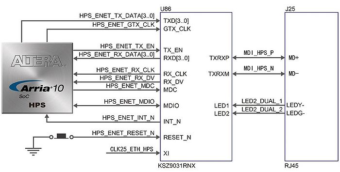
5.2 Gigabit Ethernet
The board supports Gigabit Ethernet transfer by an external Micrel KSZ9031RNX PHY chip and HPS Ethernet MAC function. The KSZ9031RNX chip with integrated 10/100/1000 Mbps Gigabit Ethernet transceiver also supports RGMII MAC interface. Figure 5-1 shows the connections between the HPS, Gigabit Ethernet PHY, and RJ-45 connector. The pin assignment associated with Gigabit Ethernet interface is listed in Table 5-2. More information about the KSZ9031RNX PHY chip and its datasheet, as well as the application notes, is available on the manufacturer’s website.
- Figure 5-1 Connections between the HPS and Gigabit Ethernet
- Table 5-2 Pin Assignment of Gigabit Ethernet PHY

Signal Name FPGA Pin Number Description I/O Standard HPS_ENET_GTX_CLK PIN_F25 GMII Transmit Clock 1.8V HPS_ENET_MDC PIN_D24 Management Data Clock Reference 1.8V HPS_ENET_MDIO PIN_C24 Management Data 1.8V HPS_ENET_RX_CLK PIN_K22 GMII and MII receive clock 1.8V HPS_ENET_RX_DATA[0] PIN_H23 GMII and MII receive data[0] 1.8V HPS_ENET_RX_DATA[1] PIN_J23 GMII and MII receive data[1] 1.8V HPS_ENET_RX_DATA[2] PIN_F24 GMII and MII receive data[2] 1.8V HPS_ENET_RX_DATA[3] PIN_G24 GMII and MII receive data[3] 1.8V HPS_ENET_RX_DV PIN_L22 GMII and MII receive data valid 1.8V HPS_ENET_TX_DATA[0] PIN_H24 MII transmit data[0] 1.8V HPS_ENET_TX_DATA[1] PIN_J24 MII transmit data[1] 1.8V HPS_ENET_TX_DATA[2] PIN_M22 MII transmit data[2] 1.8V HPS_ENET_TX_DATA[3] PIN_M21 MII transmit data[3] 1.8V HPS_ENET_TX_EN PIN_G25 GMII and MII transmit enable 1.8V
There are four LEDs, two green LEDs(LEDG) and two yellow LEDs(LEDY), which represent the status of Ethernet PHY (KSZ9031RNX). The LED control signals are connected to the LEDs on the RJ45 connector. The state and definition of LEDG and LEDY are listed in Table 5-3. For instance, the connection from board to Gigabit Ethernet is established once the LEDG lights on.
- Table 5-3 State and Definition of LED Mode Pins
LED (State) LED (Definition) Link /Activity LEDG LEDY LEDG LEDY H H OFF OFF Link off L H ON OFF 1000 Link / No Activity Toggle H Blinking OFF 1000 Link / Activity (RX, TX) H L OFF ON 100 Link / No Activity H Toggle OFF Blinking 100 Link / Activity (RX, TX) L L ON ON 10 Link/ No Activity Toggle Toggle Blinking Blinking 10 Link / Activity (RX, TX)
5.3 UART to USB
The board has one UART interface connected for communication with the HPS. This interface doesn’t support HW flow control signals. The physical interface is implemented by UART-USB onboard bridge from a FT232R chip to the host with an USB Mini-B connector. More information about the chip is available on the manufacturer’s website, or in the directory \Datasheets\UART TO USB of DE10-Advanced system CD. Figure 5-2 shows the connections between the HPS, FT232R chip, and the USB Mini-B connector. Table 5-4 lists the pin assignment of UART interface connected to the HPS.
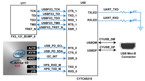
- Figure 5-2 Connections between the HPS and USB Mini-B connector
- Table 5-4 Pin Assignment of UART Interface

Signal Name FPGA Pin Number Description I/O Standard USB_PD_SCL PIN_AJ19 I2C Serial Clock 1.8V USB_PD_SDA PIN_AV16 I2C Serial Data 1.8V I2C_INT PIN_AH27 inter-integrated circuit 1.8V HPS_RXD_M PIN_L20 HPS UART Receiver 1.8V HPS_TXD_M PIN_J19 HPS UART Transmitter 1.8V
5.4 Micro SD Card Socket
The board supports Micro SD card interface with x4 data lines. It serves not only an external storage for the HPS, but also an alternative boot option for DE10-Standard board. Figure 5-3 shows signals connected between the HPS and Micro SD card socket. Table 5-5 lists the pin assignment of Micro SD card socket to the HPS.
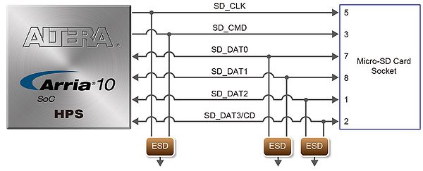
- Figure 5-3 Connections between the FPGA and SD card socket

- Table 5-5 Pin Assignment of Micro SD Card Socket
Signal Name FPGA Pin Number Description I/O Standard SD_CLK PIN_K18 HPS SD Clock 1.8V SD_CMD PIN_F22 HPS SD Command Line 1.8V SD_DATA0 PIN_J18 HPS SD Data[0] 1.8V SD_DATA1 PIN_E23 HPS SD Data[1] 1.8V SD_DATA2 PIN_G21 HPS SD Data[2] 1.8V SD_DATA3 PIN_H21 HPS SD Data[3] 1.8V
5.5 USB OTG
The board has one USB 2.0 type-A port with a SMSC USB3320 controller. The SMSC USB3320 device in 32-pin QFN RoHS Compliant package. This device supports UTMI+ Low Pin Interface (ULPI), which communicates with the USB 2.0 controller in HPS. The PHY operates in Host mode by connecting the ID pin of USB3320 to ground. When operating in Host mode, the device is powered by the USB type-A port. Figure 5-4 shows the connections of USB PTG PHY to the HPS. Table 5-6 lists the pin assignment of USB OTG PHY to the HPS.
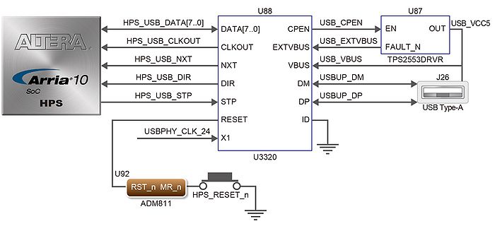
- Figure 5-4 Connections between the HPS and USB OTG PHY

- Table 5-6 Pin Assignment of USB OTG PHY
Signal Name FPGA Pin Number Description I/O Standard HPS_USB_CLKOUT PIN_L25 60MHz Reference Clock Output 1.8V HPS_USB_DATA[0] PIN_K25 HPS USB_DATA[0] 1.8V HPS_USB_DATA[1] PIN_G26 HPS USB_DATA[1] 1.8V HPS_USB_DATA[2] PIN_E27 HPS USB_DATA[2] 1.8V HPS_USB_DATA[3] PIN_F27 HPS USB_DATA[3] 1.8V HPS_USB_DATA[4] PIN_L24 HPS USB_DATA[4] 1.8V HPS_USB_DATA[5] PIN_M24 HPS USB_DATA[5] 1.8V HPS_USB_DATA[6] PIN_K23 HPS USB_DATA[6] 1.8V HPS_USB_DATA[7] PIN_L23 HPS USB_DATA[7] 1.8V HPS_USB_DIR PIN_J25 Direction of the Data Bus 1.8V HPS_USB_NXT PIN_H26 Direction of the Data Bus 1.8V HPS_USB_STP PIN_M25 Stop Data Stream on the Bus 1.8V
5.6 GPIO Header
There is a 2x5 pin header(2.54mm) on the DE10-Advanced which connected to six FPGA HPS farbric GPIOs.These I/Os can be used as GPIO that are directly controlled by HPS. Or it can be used as SPI interface (HPS_DIO[11:8]), using the SPI master controller in HPS to communicate with other SPI devices.
Chapter 6 System Clocks
Figure 6-1 shows the Clock Net connected to FPGA on DE 10-Advanced.
The Si5350c provides the fixed system frequencies to FPGA, HPS and other important components. There are four 50 MHz connected to the dedicated clock pins of the FPGA, which can be used by PLL for clock multiplier or frequency division. In addition, there are Programmable PLL (CDCM6280, BGA/FXXXXX) available for providing the clocks to the peripherals on the board, such as HDMI and communication interfaces. There is a default clock when power on, it also supports the users to change the frequency via I2C interface for special requirement.

- Figure 6-1 System Clock in the DE10-Advanced

- Figure 6-2 shows the default settings for different PLLs
Chapter 7 Power and Reset
7.1 Power Tree
Figure 7-1 is DE10-Advanced Power Tree.
DE10-Advanced can be supplied by the 12V power adapter in the package, or external connecting to USB type C as power supply.
The maximum load of the system supports is 60W (FPGA usage is 92 %) by our test.
However, please note that it is different FPGA efficient for different project. This result is only for a reference.

Figure 7-1 The power tree of the DE10-advanced
Chapter 8 DE10-Advanced System Builder
This chapter describes how users can create a custom design project with the tool named DE10-Advanced System Builder.
8.1 Introduction
The System Builder is a Windows based software utility. It is designed to help users create a Quartus Prime project for the FPGA board within minutes. The Quartus Prime project files generated include:
- Quartus Prime Project File (.qpf)
- Quartus Prime Setting File (.qsf)
- Top-Level Design File (.v)
- Synopsis Design Constraints file (.sdc)
- Pin Assignment Document (.htm)
The above files generated by the DE10-Advanced System Builder can also prevent occurrence of situations that are prone to compilation error when users manually edit the top-level design file or place pin assignment. The common mistakes users may encounter are:
- Board is damaged due to incorrect bank voltage setting or pin assignment
- Board is malfunctioned because of wrong device chosen, declaration of pin location or direction is incorrect or forgotten
- Performance degradation due to improper pin assignment
8.2 General Design Flow
This section will introduce the general design flow to build a project for the FPGA board via the System Builder. The general design flow is illustrated in the Figure 8-1.
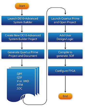
- Figure 8-1 The general design flow of building a project
- Figure 8-1 The general design flow of building a project

Users should launch System Builder and create a new project according to their design requirements. When users complete the settings, the System Builder will generate two major files which include top-level design file (.v) and the Quartus Prime setting file(.qsf).
The top-level design file contains top-level Verilog wrapper for users to add their own design/logic. The Quartus Prime setting file contains information such as FPGA device type, top-level pin assignment, and I/O standard for each user-defined I/O pin.
Finally, Quartus Prime programmer must be used to download SOF file to the FPGA board using JTAG interface.
8.3 Using DE10-Advanced System Builder
This section provides the detailed procedures on how to use the DE10-Advanced System Builder.
8.3.1 Install and Launch the DE10-Advanced System Builder
The DE10-Advanced System Builder is located in the directory: “Tools\SystemBuilder” of the DE10-Advanced System CD. Users can copy the entire folder to a host computer without installing the utility. A window will pop up, as shown in Figure 8-2, after executing the DE10-Advanced SystemBuilder.exe on the host computer.
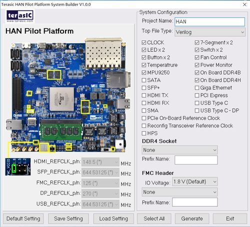
- Figure 8-2 The GUI of DE10-Advanced System Builder

8.3.2 Enter Project Name
Enter the project name in the circled area, as shown in Figure 8-3. The project name typed in will be assigned automatically as the name of your top-level design entity.
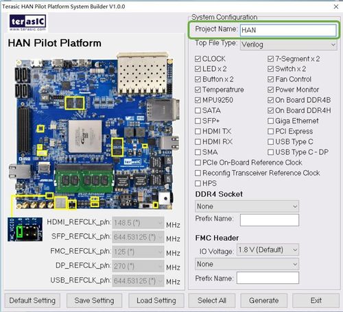
- Figure 8-3 Project Name in the System Builder window

8.3.3 Select Top File Type
The system builder can generate Verilog or VHDL Quartus top file according to users’requirement. Users can select their desired file type in the Top File Type list-box shown in Figure 8-4.

- Figure 8-4 Top File Type in the System Builder window

8.3.4 System Configuration
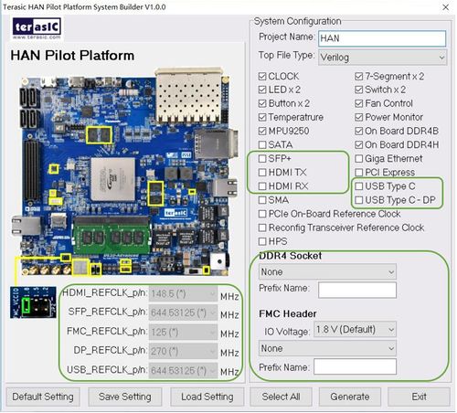
Users are given the flexibility of enabling their choices of components connected to the FPGA under System Configuration, as shown in Figure 8-5. Each component of the FPGA board is listed to be enabled or disabled according to users’ needs. If a component is enabled, the System Builder will automatically generate the associated pin assignments including its pin name, pin location, pin direction, and I/O standards. Note: The pin assignments for some components (e.g. DDR4 and SFP+) require associated controller codes in the Quartus project or it would result in compilation error. Hence please do not select them if they are not needed in the design.
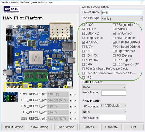
- Figure 8-5 System Configuration group

8.3.5 FMC Expansion
If users connect any compatible Terasic FMC-based daughter cards to the FMC connectoron DE10-Advanced, the DE10-Advanced System Builder can generate a project that include the corresponding module, as shown in Figure 8-6. It will also generate the associated pin assignment automatically, including pin name, pin location, pin direction, and I/O standard.
The “Prefix Name” is an optional feature that denotes the pin name of the daughter card assigned in your design. Users may leave this field blank.

- Figure 8-6 FMC expansion group

8.3.6 Programmable Clock Generator
There are some oscillators on-board (Si5350C,CDCM6208) that provide reference clocks for the following signals:
- HDMI_REFCLK
- SFP_REFCLK
- FMC_REFCLK
- DP_REFCLK
- USB_REFCLK
To use these clock, users can select the desired frequency on the Programmable Oscillator group, as shown in Figure 8-7. DDR4, or SFP+ must be checked before users can start to specify the desired frequency in the programmable oscillators. As the Quartus project is created, System Builder automatically generates the associated controller according to users’ desired frequency in Verilog which facilitates users’ implementation as no additional control code is required to configure the programmable oscillator.
Note: If users need to dynamically change the frequency, they would need to modify the generated control code themselves.
- Figure 8-7 External programmable oscillators

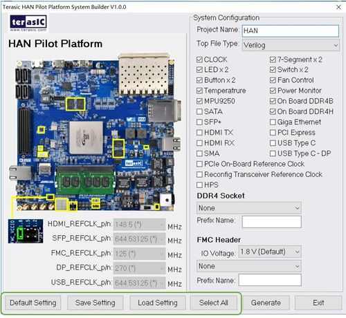
8.3.7 Project Setting Management
The System Builder also provides functions to restore default setting, load a setting, and save board configuration file, as shown in Figure 8-8. Users can save the current board configuration information into a .cfg file and load it into the System Builder.
- Figure 8-8 Project Settings

8.3.8 Project Generation
When users press the Generate button, the DE10-Advanced System Builder will generate the corresponding Quartus Prime files and documents as listed in Table 8‑1.
- Table 8-1 The file generated by DE10-Advanced System Builder
No. File Name Descriptions 1 <Project name>.v Top Verilog Quartus Prime File 2 <Project name>.qpf Quartus Prime Project File 3 <Project name>.qsf Quartus Prime Setting File 4 <Project name>.sdc Quartus Prime Synopsis Design Constraints File 5 <Project name>.htm Pin Assignment Document
Users can use Quartus Prime software to add custom logic into the project and compile the project to generate the SRAM Object File. (.sof).