DE10-Advanced revC demo: PCIe Reference Design - DDR4 Linux
From Terasic Wiki
The application reference design shows how to add DDR4 Memory Controllers for DDR4-A SODIMM and on board DDR4-B into the PCIe Quartus project based on the PCIe_Fundamental Quartus project and perform 4GB data DMA for both SODIMM. Also, this demo shows how to call “PCIE_ConfigRead32” API to check PCIe link status.
Contents |
Demonstration Files Location
The demo file is located in the batch folder: CDROM/Demonstrations/ PCIe_DDR4/demo_batch
The folder includes following files:
- FPGA Configuration File: PCIe_DDR4sof
- Download Batch file: test.sh
- Linux Application Software folder : linux_app, includes
- PCIE_DDR4
- terasic_pcie_qsys.so
Demonstration Setup
- Install DDR4 2400 4GB SODIMM on the FPGA board.
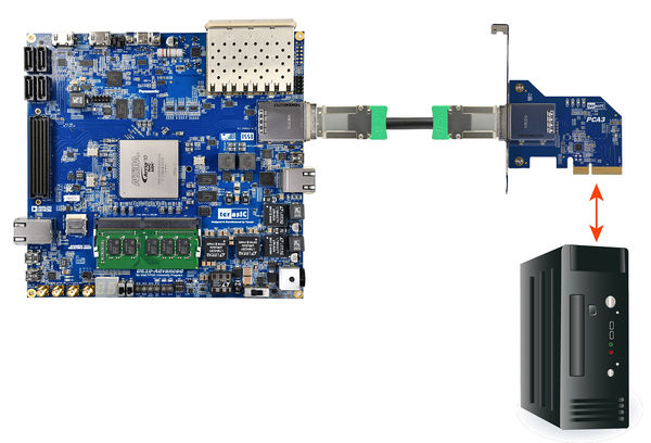
- Install the FPGA board on your PC as shown in Figure1-1.
-
- Figure 1-1 FPGA board connect to PC
- Open a terminal and use "cd" command to goto "CDROM/Demonstrations/PCIe_Fundamental/demo_batch".
- Set QUARTUS_ROOTDIR variable pointing to the Quartus installation path. Set QUARTUS_ROOTDIR variable by tying the following commands in terminal. Replace /home/centos/intelFPGA/18.0/quartus to your quartus installation path.
- export QUARTUS_ROOTDIR=/home/centos/intelFPGA/18.0/quartus
- Execute "sudo -E sh test.sh" command to configure the FPGA
- Restart Linux
- Install PCIe driver.
- Make sure the Linux has detected the FPGA Board.
- Goto linux_app folder, execute PCIE_DDR4. A menu will appear as shown in Figure 1-2.
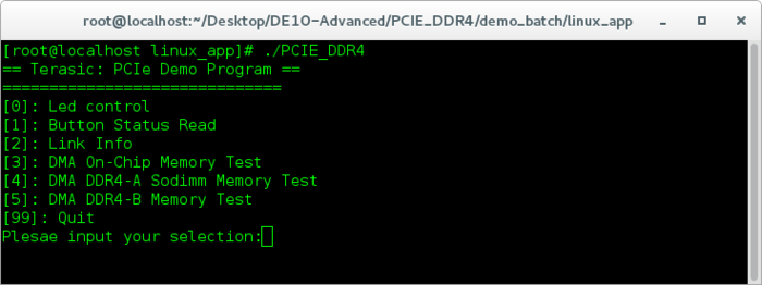
- Figure 1-2 Screenshot of Program Menu
- Type 2 followed by an ENTER key to select Link Info item. The PCIe link information will be shown as in Figure 1-3. Gen3 link speed and x8 link width are expected.
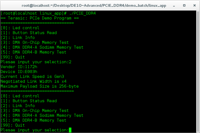
- Figure 1-3 Screenshot of Link Info
- Type 3 followed by an ENTER key to select DMA On-Chip Memory Test item. The DMA write and read test result will be report as shown in Figure 1-4.
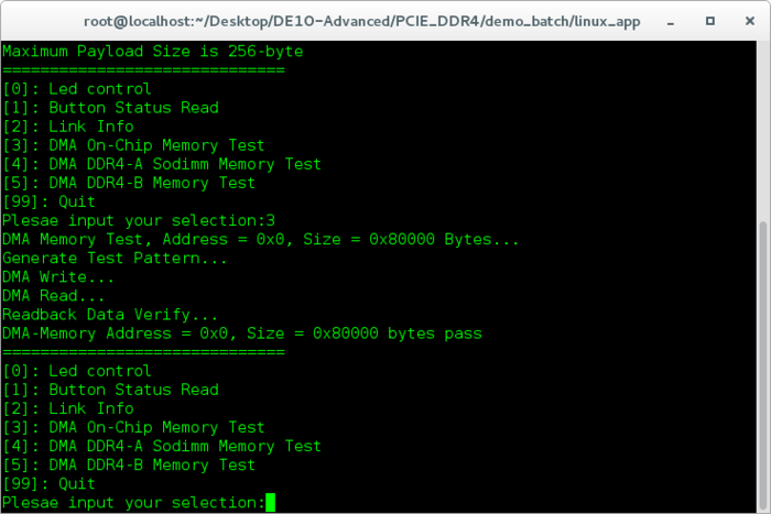
- Figure 1-4 Screenshot of On-Chip Memory DMA Test Result
- Type 4 followed by an ENTER key to select DMA DDR4-A SODIMM Memory Test item. The DMA write and read test result will be report as shown in Figure 1-5.
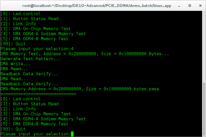
- Figure 1-5 Screenshot of DDR4-A SOSIMM Memory DAM Test Result
- Type 5 followed by an ENTER key to select DMA DDR4-B Memory Test item. The DMA write and read test result will be report as shown in Figure 1-6.
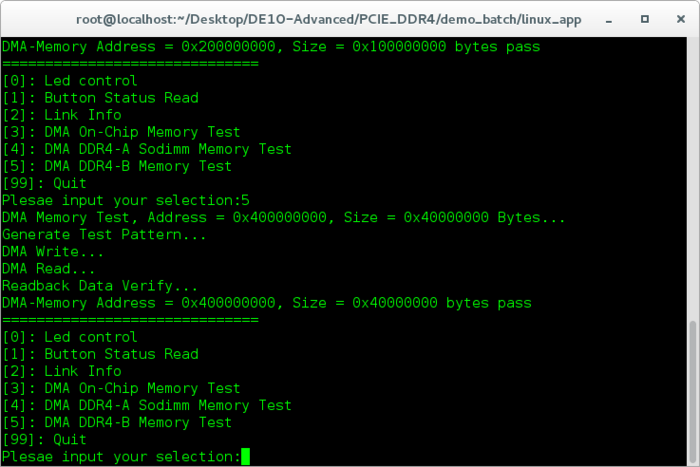
- Figure 1-6 Screenshot of DDR4-B SOSIMM Memory DAM Test Result
- Type 99 followed by an ENTER key to exit this test program.


Development Tools
- Quartus Prime 18.0 Standard Edition
- GNU Compiler Collection, Version 4.8 is recommended
Demonstration Source Code Location
- Quartus Project: Demonstrations/PCIE_DDR4
- C++ Project: Demonstrations/PCIe_SW_KIT/Linux/PCIe_DDR4
FPGA Application Design
Figure 1-7 shows the system block diagram in the FPGA system. In the Qsys, Altera PIO controller is used to control the LED and monitor the Button Status, and the On-Chip memory is used for performing DMA testing. The PIO controllers and the On-Chip memory are connected to the PCI Express Hard IP controller through the Memory-Mapped Interface.

- Figure 1-7 Hardware block diagram of the PCIe_DDR4 reference design
Linux Based Application Software Design
The application software project is built by GNU Toolchain. The project includes the following major files:
NAME Description PCIE_FUNDAMENTAL.cpp Main program PCIE.c Implement dynamically load for terasic_pcie_qsys.so library file PCIE.h TERASIC_PCIE_AVMM.h SDK library file, defines constant and data structure
The main program PCIE_DDR4.cpp includes the header file "PCIE.h" and defines the controller address according to the FPGA design.

The base address of BUTTON and LED controllers are 0x4000010 and 0x4000020 based on PCIE_BAR4, in respectively. The on-chip memory base address is 0x00000000 relative to the DMA controller. The above definition is the same as those in PCIe Fundamental demo.
Before accessing the FPGA through PCI Express, the application first calls PCIE_Load to dynamically load the terasic_pcie_qsys.so. Then, it call PCIE_Open to open the PCI Express driver. The constant DEFAULT_PCIE_VID and DEFAULT_PCIE_DID used in PCIE_Open are defined in TERASIC_PCIE_AVMM.h. If developer change the Vendor ID and Device ID and PCI Express IP, they also need to change the ID value define in TERASIC_PCIE_AVMM.h. If the return value of PCIE_Open is zero, it means the driver cannot be accessed successfully. In this case, please make sure:
- The FPGA is configured with the associated bit-stream file and the host is rebooted.
- The PCI express driver is loaded successfully.
The LED control is implemented by calling PCIE_Write32 API, as shown below:
![]()
The button status query is implemented by calling the PCIE_Read32 API, as shown below:
![]()
The memory-mapped memory read and write test is implemented by PCIE_DmaWrite and PCIE_DmaRead API, as shown below:

The PCIe link information is implemented by PCIE_ConfigRead32 API, as shown below:
