DE10-Advanced revC demo: PCIe Reference Design - Fundamental Linux
From Terasic Wiki
Contents |
Demonstration Files Location
The demo file is located in the batch folder: CDROM/Demonstrations/PCIe_Fundamental/demo_batch
The folder includes following files:
- FPGA Configuration File: PCIe_Fundamental.sof
- Download Batch file: test.sh
- Linux Application Software folder : linux_app, includes
- PCIE_FUNDAMENTAL
- terasic_pcie_qsys.so
Demonstration Setup
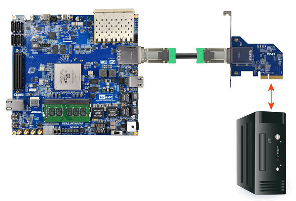
- Install the FPGA board on your PC as shown in Figure1-1.
-
- Figure 1-1 FPGA board connect to PC
- Open a terminal and use "cd" command to goto "CDROM/Demonstrations/PCIe_Fundamental/demo_batch".
- Set QUARTUS_ROOTDIR variable pointing to the Quartus installation path. Set QUARTUS_ROOTDIR variable by tying the following commands in terminal. Replace /home/centos/intelFPGA/18.0/quartus to your quartus installation path.
- export QUARTUS_ROOTDIR=/home/centos/intelFPGA/18.0/quartus
- Execute "sudo -E sh test.sh" command to configure the FPGA
- Restart Linux
- Install PCIe driver. The driver is located in the folder: CDROM/Demonstration/PCIe_SW_KIT/Linux/PCIe_Driver.
- Type “ls –l /dev/altera_pcie*” to make sure the Linux has detected the FPGA Board. If the FPGA board is detected, developers can find the /dev/altera_pcieX(where X is 0~255) in Linux file system as shown below.
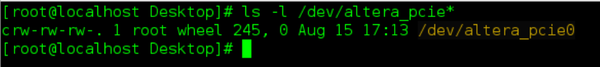 .
.
- Goto linux_app folder, execute PCIE_FUNDAMENTAL. A menu will appear as shown in Figure 1-2.
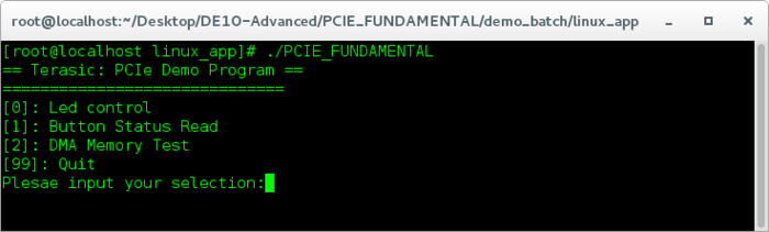
- Figure 1-2 Screenshot of Program Menu
- Type 0 followed by a ENTER key to select Led Control item, then input 3 (hex 0x03) will make all led on as shown in Figure 1-3. If input 0 (hex 0x00), all led will be turn off.
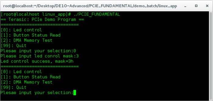
- Figure 1-3 Screenshot of LED Control
- Type 1 followed by an ENTER key to select Button Status Read item. The button status will be report as shown in Figure 1-4.
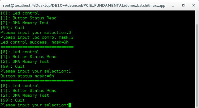
- Figure 1-4 Screenshot of Button Status Report
- Type 2 followed by an ENTER key to select DMA Testing item. The DMA test result will be report as shown in Figure 1-5.
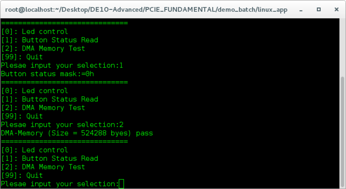
- Figure 1-5 Screenshot of DMA Memory Test Result
- Type 99 followed by an ENTER key to exit this test program


Development Tools
- Quartus Prime 18.0 Standard Edition
- GNU Compiler Collection, Version 4.8 is recommend
Demonstration Source Code Location
- Quartus Project: Demonstrations/PCIe_Fundamental
- C++ Project: Demonstrations/PCIe_SW_KIT/Linux/PCIE_FUNDAMENTAL
FPGA Application Design
Figure 8-9 shows the system block diagram in the FPGA system. In the Qsys, Altera PIO controller is used to control the LED and monitor the Button Status, and the On-Chip memory is used for performing DMA testing. The PIO controllers and the On-Chip memory are connected to the PCI Express Hard IP controller through the Memory-Mapped Interface.

- Figure 8-9 Hardware block diagram of the PCIe reference design
Linux Based Application Software Design
The application software project is built by GNU Toolchain. The project includes the following major files:</div>
NAME Description PCIE_FUNDAMENTAL.cpp Main program PCIE.c Implement dynamically load for TERAISC_PCIE_AVMM.DLL PCIE.h TERASIC_PCIE_AVMM.h SDK library file, defines constant and data structure

The base address of BUTTON and LED controllers are 0x4000010 and 0x4000020 based on PCIE_BAR4, in respectively. The on-chip memory base address is 0x00000000 relative to the DMA controller.
Before accessing the FPGA through PCI Express, the application first calls PCIE_Load to dynamically load the terasic_pcie_qsys.so. Then, it call PCIE_Open to open the PCI Express driver. The constant DEFAULT_PCIE_VID and DEFAULT_PCIE_DID used in PCIE_Open are defined in TERASIC_PCIE_AVMM.h. If developer change the Vendor ID and Device ID and PCI Express IP, they also need to change the ID value define in TERASIC_PCIE_AVMM.h. If the return value of PCIE_Open is zero, it means the driver cannot be accessed successfully. In this case, please make sure:
- The FPGA is configured with the associated bit-stream file and the host is rebooted.
- The PCI express driver is loaded successfully.
![]()
![]()
