DE10-Agilex Rev.A to Rev.B Revision List
From Terasic Wiki
Rev. A to Rev. B
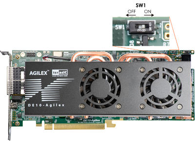
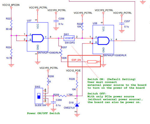
- Add Force External Power Switch (SW1) to Enable/Disable External Power Requirement when connected to the HOST PC.
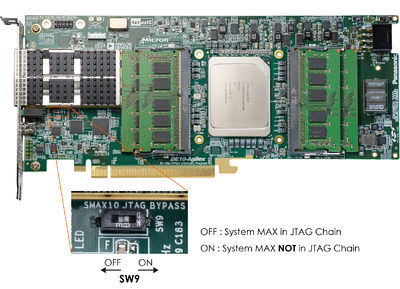
- Add System MAX10 Jtag bypass switch (SW9) for increasing JTAG scan speed.
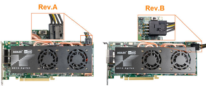
- Modify the direction of the external power connector.
- Remove DDR4 Clock Source Switch (SW5) and change the DDR4 source clock oscillator (Y2) from dual clock OSC (166.667/300.0MHz) to 33.333Mhz OSC.
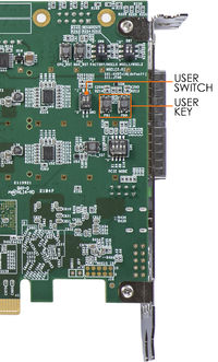
- Move the user switch and key from the front of the board to the back.
- Modify the reference clock source(Y1) of the SI5340 clock generator(U13) to TCXO to increase the quality of the QSFPDD reference clock.
- Improve the core power chip(U15, VCC_CORE) from LT4680(rev.A) to LT4700(rev.B) , the power can be improve from 60A to 100A
- Rev.B board add a 30.72Mhz OCXO(U161) but it is not installed, reserved for CPRI application.
- Add external power connection detection I/O(EXP_EN) to FPGA.
- Pin Assignment change.
| Net Name | Rev.A Pin Assignment | Rev.B Pin Assignment |
|---|---|---|
| PCIE_SMBCLK | F59 | G50 |
| PCIE_CLKREQ_n | J58 | F55 |
| PCIE_WAKE_n | G58 | J50 |
| DDR4B_SDA | H57 | B19 |
| GPIO_CLK0 | CU24 | DA22 |
| GPIO_P0 | DA22 | CY21 |
| INFO_SPI_MISO | CY21 | CU26 |
