DE2-115 FAQ English version
From Terasic Wiki
-
- Q:What is the function of the JP4 on DE2-115?
- A:The JP4 on DE2-115 is designed and reserved for MIPS CPU; users can also use it for general FPGA IO design application.
-
- Q:What OS does the USB driver of DE2-115 support
- A:DE2-115 is equipped with two types of USB chips; they are NXP ISP1362 and Cyptess cy7c67200. The DE2-115 currently available comes with Cypress cy7c67200. The driver provided in the system CD supports windows 7 for 32 /64bit and Windows XP for 32/64bit.
-
- Q:What can you do when failing to download the .sof file into the FPGA of the DE2-115 and encountering the situation as shown below??
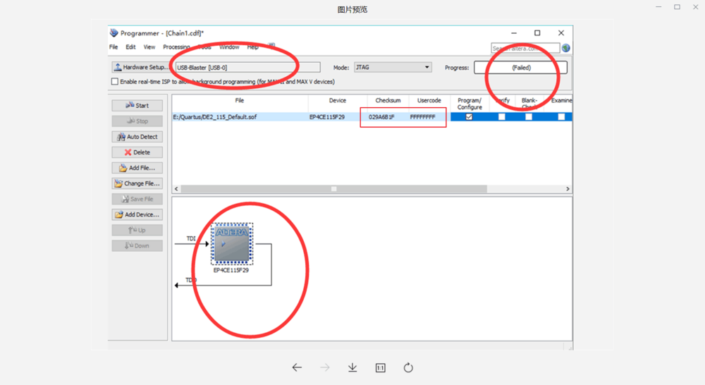
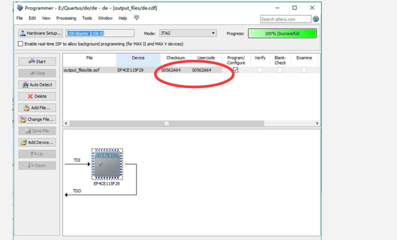
- A:Normally the Checksum and Usercode should be the same (as shown below). From the previous picture, we can see the USB-Blaster hardware exists, but the Checksum and the Usercode are different. In this situation, please make sure your JP2 jumper setting and the JTAG-Chain are correct (for more details, please refer to DE2_115_User_manual.pdf, page No. 30)..
-
- Q:How can you troubleshoot the problems first when failed to download the .sof file to the DE2-115?
- A:You can start with the followin:
- Check the SW19 and make sure it’s set to “RUN”
- Have a test to see if DE2-115 would run the default code when power up.
- Check the JP3 jumper setting. If DE2-115 is without any daughter cards connected, pin 1 and pin 2 of JP3 should be shorted; while if the JTAG signal needs to be connected to the daughter card, pin 2 and pin 3 of JP3 should be shorted.
- Open the Quartus Programmer window and click on the "Hardware Setup." button to see if there is a USB Blaster hardware shows up; then click "Auto Detect" to see if the Quartus software reports an error.
-
- Q:What is the maximum transmission rate (MB/s) for the DE2-115 network interface?
- A:The projects provided on Terasic official web are made based on Nios by using Altera’s TSE IP. We’ve got a result which is approximately 100~200 Mb/s at the application level. Users can also design or optimize their own projects to speed up the transmission.
-
- Q:What is the maximum power consumption of DE2-115? What is the maximum frequency of the square wave that its GPIO interface can output? What is the maximum square wave frequency that LVDS on its HSMC interface can output?
- A:The maximum power consumption of DE2-115 is about 15W. The square wave frequency of the GPIO output is suggested not exceed 7M. The LVDS is emulated LVDS, not the real LVDS, and the maximum frequency is about 500M.
-
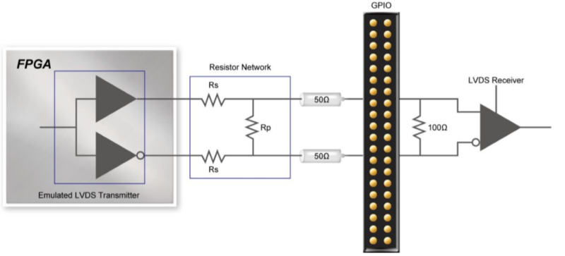
- Q:Can the GPIO on DE2-115 be used as an LVDS transmitter (TX) and receiver (RX)?
- A:Theoretically, the GPIO on DE2-115 can either be used as an LVDS transmitter (TX) or be used as a receiver (RX). And in practice, GPIO can exactly be used and simulated as a receiver, but we don’t recommend to do so because the protection circuits will significantly slow down the transmission speed.
- When you want to use GPIO as an LVDS transmitter, please note that in this situation you need to add an extra resistor network (as shown below). Normally the default resistance of Rs is 47 ohms, and Rp is not installed by default. When these I/Os are used as the LVDS transmitter, you need to install a 120 ohm resistor in the Rs position and a 170 ohm resistor in the Rp position. Besides, in Quartus II, the corresponding I/Os differential pairs must be set to LVDS_E_3R. For more details, please consult the DE2-115 user manual available on Terasic website.
-
- Q:When making a connection between DE2-115 and the PC via an RS-232 cable to run Control Panel, why can’t the UART properly work and can’t find a new device in Device Manager?
- A:The UART cannot transmit and receive; this may be a problem with the TX and RX signal of the RS-232 cable. Please prepare a multimeter, and then switch to ohms grades for measurement. Please confirm whether the pin 2 of the male / female connector on the RS-232 cable is connected to each other (resistance 0 ohm), and whether the pin 3 of the connector is connected to each other
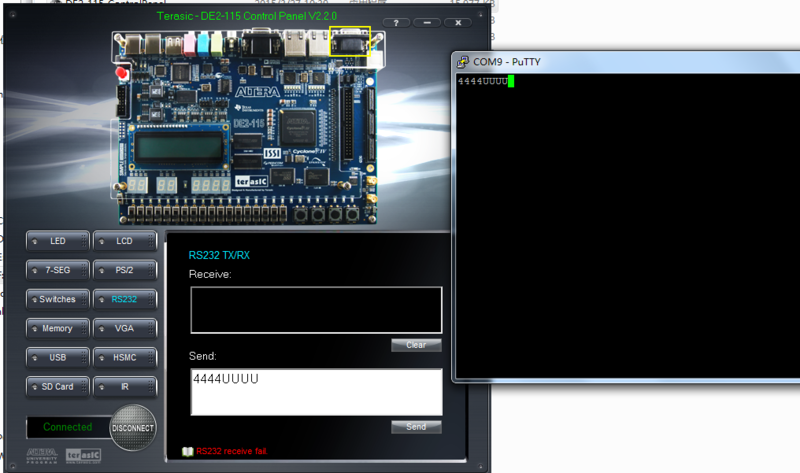
- As for question "why can’t find a new device in Device Manager", in fact, the device manager already displays the default COM port of the PC, so no new device will appear, (as shown in the figure below), you can directly target the COM Port Configuration, PC does not necessarily appear new device.
- Further explanation on data transmission: sending data in Control Panel interface, and receiving data in putty interface; and then sending data in putty interface and receiving data in Control Panel interface (as shown below).
-
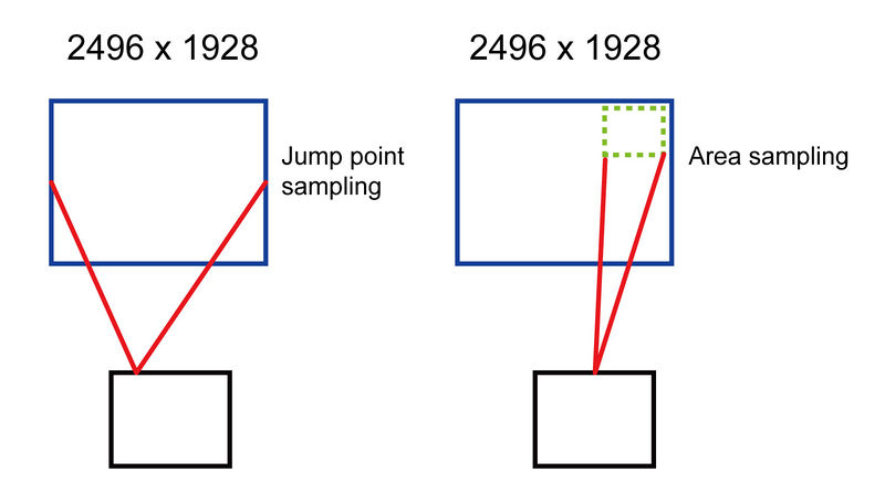
- Q: Why does the design of SDRAM in the demonstration DE2_115_CAMERA only save half of the data? What is the principle of the picture enlargement function in this project?
- A:The SDRAM only saves half of the data in this demonstration, because it is created based on the design of other projects, and users can design again according to their own needs. About the amplification principle of this demo
- For image enlargement questions: 1).The mode without magnification is to sample the 800x600 image from the pixel jump point of the 2496 x 1928 image from the camera. 2). The enlargement mode is area sampling, for example, 0 ~ 800 pixel (width), so the image effect taken out on the right will be the effect of image enlargement.
-
- Q: How to control the EEPROM on DE2-115? Are there any references?
- A: Users can use I2C to control the EEPROM on DE2-115. No corresponding examples for DE2-115 can be provided for reference but users can consult the example in DE0-Nano’s system CD under file : DE0-Nano_V.1.2.0_CDROM\Demonstration\DE0_Nano_SOPC_DEMO; this example involves the code of how to control the EEPROM (Download Link : https://www.terasic.com.tw/cgi-bin/page/archive.pl?Language=English&CategoryNo=139&No=593&PartNo=4 )


