HERO Doucment Hardware Manual English
From Terasic Wiki
Contents |
Chapter 1 Introduction
1.1 Overview
The HERO platform (the Heterogeneous Extensible Robot Open Platform) is a low-power, high-performance, small-volume heterogeneous system platform solution for intelligent robots (including service robots, medical robots, self-driving cars, etc.). In this platform, the CPU acts as a control center, paired with FPGAs to provide efficient performance. The complete HERO hardware system features an Intel® CoreTM processor with an Intel Arria 10 GX Series 1150 FPGA as a heterogeneous accelerator.
The traditional FPGA programming has proved problematic to most software engineers, and the HERO platform has provided a solution for everyone. In addition to the traditional professional programming model, the HERO platform’s customized BSP (Board Support Package) also supports OpenCL-based flow development, providing a friendly programming interface for a wide range of algorithms and software programming for software engineers. For a customized system to support OpenCL flow, it requires FPGA hardware to provide complete data and control paths other than compatible software from the host. The OpenCL kernel can then be loaded dynamically in real time and run on the FPGA platform. To support OpenCL Flow, the full FPGA board support package has been ported to the HERO platform and is available as an integral part of the HERO SDK. The FPGA logic part of the existing HERO SDK BSP mainly includes a high-speed communication interface PCIe IP core, a memory DMA controller, an off-chip high-speed memory DDR4 interface, and a communication interface with the FPGA internal module. If users want to increase the speed of communications between the FPGA and the external interface, the HERO platform also has a corresponding BSP reference design that guides customers to implement a variety of flexible external interfaces for better and faster communication.
The HERO platform has broad application prospects. Take the service robot as an example, its main role is to help people complete tasks and actions. To achieve this goal, R&D personnel need to implement a variety of complex application control techniques on the robot, including vision, positioning, motion, and grabbing. FPGAs can be of great value in these critical applications, making the processing of complex algorithms efficient and real-time, giving users a good experience.
1.2 Technical Specifications
Hero platform is composed of two boards, one is the CPU host system, the other is FPGA acceleration system (see Figure 1-1). The two boards use PCIe interface to connect and communicate each other to complete the work of FPGA assisted CPU implementing various calculation functions and algorithm accelerations. The FPGA system using Intel Arria10 FPGA PCIe card version. The following will introduce the two main systems parameter specifications in details:
- CPU main System
- Processor: Intel® Core™ i5-7260U / Intel® Core™ i7-7567U (according to the customer’s order request)
- Memory: DDR4-2133 1.2V SO-DIMM 8GB
- Hard disk: Sata SSD 256G
- The graphics card
- Integrated graphics
- Graphic output: HDMI 2.0a; USB-C (DP1.2)
- Peripheral Interface
- USB Type C Port x1
- Thunderbolt™ 3 (40Gbps)
- USB 3.1 Gen 2 (10Gbps)
- DisplayPort (DP 1.2)
- USB 3.0/2.0 Port x2
- LAN: Gigabit (10/100/1000 Mb/s) LAN
- Wireless: Intel® Wireless-AC 8265 + Bluetooth 4.2
- FPGA Acceleration system
- FPGA: Intel Arria 10 GX FPGA (10AX115S2F45I1SG)
- FPGA Configuration Circuit
- On-Board USB Blaster II or JTAG header for FPGA programming
- Fast Passive Parallel (FPPx32) configuration via MAX II CPLD and flash memory
- memory
- 256 MB Flash
- 2 GB ddr4 - 2400 x 64 bit
- Communication and Expansion
- PCI Express (PCIe) x8 edge connector
- USB 3.0 Host/Device
- Gigabit Ethernet
- UART / CAN / SPI / I2C
- General user input / output:
- 8 LEDs
- 3 Push-buttons
- 8 DIP Switch
- clock
- 50/100/125MHz fixed clock
- programmable PLL
- System Monitor and Control
- Temperature sensor
- Power Monitor
Chapter 2 System Interface Introduction and Description
2.1. Overview
The HERO platform is composed of CPU host system and FPGA accelerator card. As shown in figure 2-1, external interfaces on the HERO platform are also divided into two categories. The peripheral interfaces marked in orange line are CPU host system interface, such as HDMI and USB interfaces. With the two interfaces, operating system running on the CPU host system can use mouse or screen output function.
The peripheral interfaces marked in blue line are FPGA accelerator card interface. With these interfaces, FPGA acceleration card can have the ability to expand peripherals. For example, connecting to ethernet the FPGA acceleration card can have communication ability to deal with network function. But these interfaces require users to implement corresponding design in FPGA. The default code doesn’t include these designs.
In addition, it should be noted that these two systems are independent, for example, the Ethernet is connected to the FPGA acceleration card, then, the FPGA acceleration card can have network ability but the CPU host system can’t. Similarly, plug the USB mouse on the FPGA acceleration card, the FPGA acceleration card can detect the mouse, the CPU host system can’t.

Figure 2-1 The Main Interfaces on HERO platform
Next, we will introduce the power supply on HERO platform and the interface of CPU host system. The FPGA accelerator card interfaces will be described in Chapter 3.
2.2 12V System Power Input and FPGA Power Switch
Figure 2-2 shows the power input port of HERO platform and FPGA power switch. DC 12V power supplier is required to supply the power.The FPGA power switch is the FPGA accelerator card power switch. Please start this switch first to powered and configured the FPGA, and later, power on the CPU system, then, the CPU system can detect the FPGA accelerator card device.

Figure 2-2 12V System Power Input and FPGA Power Switch
2.3 CPU host system Power button
Figure 2-3 is the power button of the CPU host system, and this button can be pressed to turn on the CPU host system. As in the most PC machines, when the CPU host system is turned on (blue light will appear on the button), pressing this button for four seconds will force the system power to shut down. And press one time, the operation system will appear restart options.

Figure 2-3 CPU host system Power button
2.4 CPU host system interface
This section describes the peripheral interfaces of the CPU host system.
High Definition Multimedia Interface* (HDMI*)

Figure 2-4 High Definition Multimedia Interface
The HDMI port supports standard, enhanced, or high definition video, plus multi-channel digital audio on a single cable. The port is compatible with all ATSC and DVB HDTV standards and supports eight full range channels at 24-bit/96 kHz audio of lossless audio formats. The maximum supported resolution is 4096 x 2160 @ 60 Hz, 24bpp. The HDMI port is compliant with the HDMI 2.0 specification.
Gigabit Ethernet LAN Port

Figure 2-4 Gigabit Ethernet LAN Port
The Ethernet Port on the CPU host system supports the following features: • Compliant with the 1 Gb/s Ethernet 802.3, 802.3u, 802.3z, 802.3ab specifications • Multi-speed operation: 10/100/1000 Mb/s • Full-duplex operation at 10/100/1000 Mb/s; Half-duplex operation at 10/100 Mb/s • Flow control support compliant with the 802.3X specification as well as the specific operation of symmetrical flow control defined by 802.3z • VLAN support compliant with the 802.3q specification
Two LEDs are built into the RJ-45 LAN connector (shown in Figure 2-5).

Figure 2-5 Two LEDs on RJ-45 LAN connector
Table 2-1 describes the LED states when the board is powered up and the LAN subsystem is operating.
Table 2-1
LED LED Color LED State Condition Link Green OFF LAN link is not established On LAN link is established Blinking LAN activity is accurring Data Rate Green/Yellow Off 10Mb/s data rate is selected Green 100Mb/s data rate is selected Yellow 1000Mb/s data rate is selected
USB 3.0 Ports
The CPU system of HERO platform provides two USB 3.0 ports, as shown in figure below. The maximum current for each port is 900 mA.
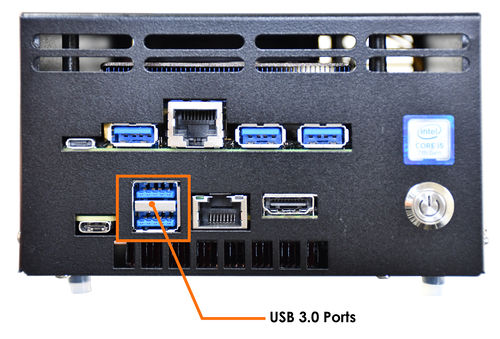
- Figure 2-6 Hero USB 3.0 Ports

USB Type-C connector
The port supports Thunderbolt™ 3 with up to 40Gbps of data throughput, one 4k (60Hz) monitor output, USB3.1 (Gen 2) connection and charging capabilities up to 5V at 3A.
It also supports DisplayPort 1.2 specification for display connections between consumer electronics devices such as high definition optical disc players, set top boxes, and TV displays. The maximum supported resolution is 4096 x 2304 @ 60 Hz, 24bpp.
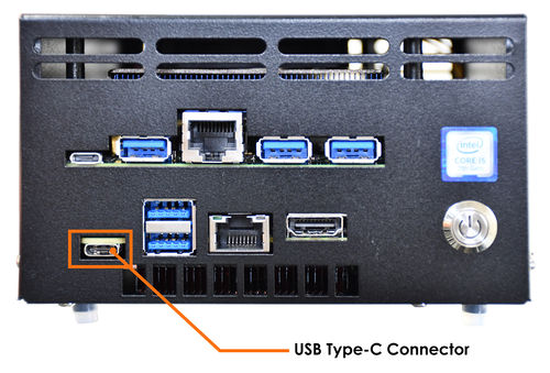
- Figure 2-7 Hero USB Type-C Connector

Chapter 3 FPGA Accelerator Card
3.1 FPGA Accelerator Card Introduction
The HERO platform embedded FPGA accelerator card which is used to implement hardware calculation acceleration function with the CPU system. Nowadays, with the help of so many development tool platforms, using FPGA card for acceleration is no longer time-consuming.
In the field of AI (Artificial Intelligence) applications, the OpenVINO toolkit provides excellent development environment. The FPGA accelerator card plays a role of terminal deployment unit, the user-trained model is inferred by the OpenVINO toolkit, finally it will be deployed to the FPGA accelerator card to realize the acceleration function of image recognition algorithm.
Users can also use the FPGA accelerator card for developing OpenCL applications. Through the complete FPGA Board Support Package, the OpenCL tool can automatically convert user’s OpenCL kernel function into a customized FPGA hardware accelerator, add interface IP, build interconnection logic and generate FPGA configuring files.System developers and programmers who are familiar with C can quickly and easily develop high-performance, high-efficiency and FPGA-based applications in high-level software environments.
Of course, users can also develop various acceleration logic in FPGA by themselves if they have strong FPGA design ability, to achieve the purpose of hardware acceleration for special applications.
To operate the supported toolkit (OpenVINO or OpenCL), the FPGA accelerator card usually requires the corresponding interface logic, such as the PCIe interface, to be configured at least when the system is turned on, then the data transmission can be conducted with the CPU host system.
Therefore, when the CPU system is turned on, the FPGA device in the FPGA acceleration card needs to be programmed with PCIe function configuration, then it can operate normally with the CPU system.
To achieve this, firstly the flash on the FPGA accelerator card needs to programmed with the PCIe function configuration file. When the FPGA card is powered on, the system controller on the card will read the configuration file in the flash and configure the FPGA.
Or before the OS is restarted, users can download the PCIe function configuration file (.sof file), so the PCIe function of the FPGA accelerator card can be found after the system is restarted. After that, the user's application logic can be downloaded and configured by the CPU system through the PCIe interface.
If users do not find the PCIe device of the FPGA accelerator card in the OS, maybe the FPGA accelerator card has not configured with the PCIe function configuration, it is necessary to check whether the flash was programmed with correct configuration file.
3.2 FPGA accelerator card block diagram
Figure 3-1 shows the FPGA acceleration system components and the connection with the CPU system.
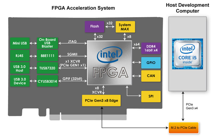
- Figure 3-1 FPGA acceleration system block diagram'

3.3 USB Blaster II Port
The USB Blaster II port is mainly used to configure the FPGA, it allows users to program the FPGA with designed configuration files (It is mainly .sof file) from the operating system using the JTAG protocol through the USB port.
Enable the FPGA to operate as the user's design. The USB Blaster II circuit is built on the FPGA accelerator card, users do not need to use the external downloader. In addition, to use the USB Blaster II circuit, the driver must be installed in the OS (The driver is in the Quartus software installation path), the driver in the HERO platform is pre-installed.
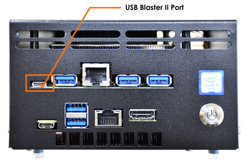
- Figure 3-2 USB Blaster II Port

Connect the USB Blaster II port to the Host computer USB port by using a mini usb cable.

Figure 3-3 Connect USB Blaster II Port to CPU Host
In the HERO platform, since the user can work with the OpenCL or OpenVNIO toolkit to configure the FPGA through the PCIe interface, there is a less time to use the USB Blaster II interface for the configuration.
The following are the main situations to use the USB blaster II port:
1. Replace or Update the flash configuration file in the FPGA accelerator, it needs to program the Flash via the USB Blaster II port.
2. If the user wants to design by himself and running the FPGA accelerator without any other toolkits, the configuration file can be downloaded into the FPGA device through the USB Blaster II port to complete the FPGA configuration as the normal FPGA board works.
3. When the version of the programmed OpenCL configuration file in Flash is different from the version of the .aocx file running, it cannot support to configure FPGA through PCIe direclty. It needs to downloaded through USB Blaster to run the FPGA in the desired state.
3.4 DDR4 Memory
The FPGA accelerator provides four DDR4 devices with a total capacity of 2GB (see figure 2-x). They can be used for data caching. The available bit width is up to 64bit and runs at 2400Mhz(FPGA speed grade: I1). The maximum bandwidth is 153.6Gbps theoretically. The I/O pin assignment of DDR4 is shown in table 2-x.

Figure 3-4 DDR4 to FPGA connection
3.5 PCIe interface
There is a PCIe Gen 3 x4 interface on the FPGA accelerator which can be used to connect to the CPU host system. Working with the built-in transceiver and integrated PCI Express hardcore IP module on the Arria 10 GX device, it can provide a fully integrated PCI Express compatibility solution.
In the HERO platform, with the assistance of OpenCL or OpenVINO toolkit, the CPU host system can configure the FPGA to complete the acceleration logic through the PCIe interface, and transmit and retrieve various data about computing the acceleration.
3.6 USB 3.0 Host Port
The FPGA accelerator retains A USB 3.0-compatible xHCI Host controller (TI :TUSB7320IRKM) to equip with two USB 3.0 Standard-A interfaces. Which is expected that the FPGA accelerator can provide two USB 3.0 Host. Note, this is a reserved function, unable to use it currently.
The interface between the TUSB7320IRKM controller and FPGA follows the PCIe x1 Gen2 protocol. So a pair of TX/RX transceiver should be used to connect these two devices.

Figure 3-5 USB Hos Port of the FPGA Accelerator
3.7 USB 3.0 Device
The FPGA accelerator is equipped with a USB3.0 controller which is the Cypress model CYUSB3014. It can be used as the USB3.0 Device and related applications of USB2.0 OTG. The user can use this port to transmit data from the FPGA to the CPU system or other hosts.

Figure 3-6 USB Blaster II Port of the FPGA Accelerator
3.8 Gigabit Ethernet
The FPGA accelerator board is configured with a 10/100/1000 gigabit Ethernet transceiver chip MARVELL88E1111.The chip is an auto-negotiated Ethernet PHY that connects to the FPGA using the default SGMII MAC interface.The transmission takes the form of LVDS I/O with a speed of 1.2Gbps. Users can place a MAC IP in the FPGA to work this accelerator communicating with external devices via Ethernet.

Figure 3-7 Ethernet Port of the FPGA Board
3.9 Clock Circuit
As shown in figure x, there is a variety of clock frequencies (OSC & on board PLL) for a variety of FPGA applications. The output frequency of PLL which is provided to FPGA transceiver bank can be changed through I2C interface for the different requirements. And the other input of fixed frequency is also being connected into the FPGA clock input dedicated pin. User can also get the frequency multiplied or frequency divided by using the FPGA internal PLL megafunction.

Figure 3-8 Clock Networks