VPX-A5SOC User Manual
From Terasic Wiki
Contents |
Chapter 1 VPX-A5SoC Development Kit
The VPX-A5SoC is a high-performance, reconfigurable 6U VPX card based on the Altera Arria V SOC FPGA. The FPGA is also embedded with dual-core ARM Cortex-A9 Processor running up to 1.05 GHz which can be used for control panel interfaces such as Ethernet, USB, SD Card and UART, etc. The board features up to 1 GB of DDR3 SDRAM as well as Flash memory for booting the FPGAs. The PCI Express ports x4 lanes in the VPX expansion plane, with up to PCI Express Gen2 (5Gbps) throughput offers a high performance interface to mainstream peripherals and I/O cards. Two VITA 57 FMC sites are provided for enhancing the board's I/O and processing capabilities. The A5-VPX-A5SoC is a powerful, feature-rich solution for the next generation of compute-intensive embedded applications.
1.1 Package Contents
The VPX-A5SoC board package includes:
- The VPX-A5SoC board
- Quick Start Guide
- TBD
1.2 VPX-A5SoC System CD
The 6U-VPX System CD contains all the documents and supporting materials associated with 6U-VPX, including the user manual, system builder, reference designs and device datasheets. Users can download this system CD from the link: http://6U-VPX.terasic.com/cd.
1.3 Getting Help
Here are the addresses where you can get help if you encounter any problems:
Terasic Technologies
9F., No.176, Sec.2, Gongdao 5th Rd, East Dist, Hsinchu City, 30070. Taiwan
Email: support@terasic.com
Tel.: +886-3-575-0880
Website: VPX-A5SoC.terasic.com
Chapter 2 Introduction of the VPX-A5SoC Board
This chapter provides an introduction to the features and design characteristics of the board.
2.1 Layout and Components
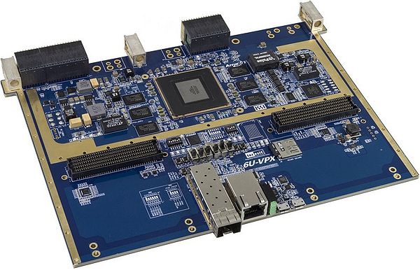
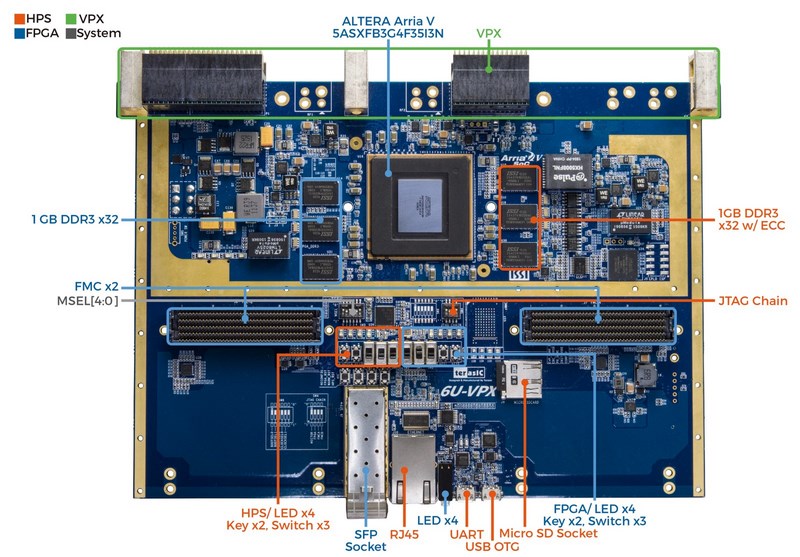
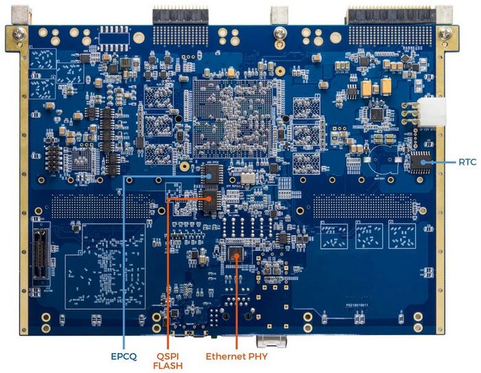
Figure 2-1 and Figure 2-2 shows a photograph of the board. It depicts the layout of the board and indicates the location of the connectors and key components.
Figure 2-1 VPX-A5SoC development board (top view)
Figure 2-2 VPX-A5SoC development board (bottom view)
The VPX-A5SoC board has many features that allow users to implement a wide range of designed circuits, from simple circuits to various multimedia projects.
The following hardware is provided on the board:
- FPGA
- EPCQ for AS-Mode FPGA configure
- Two FMC Connectors,each support transceiver x8
- 1GB DDR3 with ECC(40-bits data bus),can be extended to 2GB DDR3 by replacing with double-sized ddr3 chip
- SFP x1 connector(xcvr x1) and one differential programmable clock generator(Si570)
- User LEDs x4,KEYs x4,Switches x4,User Bracket LEDs x4
- VPX P0: JTAG,SYSRESET*,NVMRO,REF_CLK,RES_BUS(1 PPS),GA0/1/2/3/4,GAP,SM0/1/2/3(SM Bus)
- VPX P1: SYS_CON,P1-SE7(MaskableReset),one PCIe Gen2 x4
- VPX P4: UART,USB,Giga Ethernet,8 paired Differential
- 2x6 pin GPIO-Header(8 signal pins)
- HPS(Hard Processor System)
- CSEL[1:0] and BSEL[2:0](DNI,CSEL default 00,BSEL=101 default boot from sdcard)
- Two single-ended 25MHz clock source for HPS(Si5338)
- 1GB DDR3 with ECC(40-bits data bus),can be extended to 2GB DDR3 by replacing with double size ddr3 chip
- 512 Mbits QSPI Flash(for HPS configure,P/N N25Q512A83GSF40F)
- microSD Socket(eMCC shared Bus, DNI)
- RTC(Power by system power or VPX P0 3.3-AUX with Auto switching)
- User LEDs x4,KEYs x4,Switches x4
- Giga Ethernet PHY: Switchable to VPX or Front RJ45
- USB 2.0 OTG PHY: Switchable to VPX or Front micro-AB USB connector
- Two UART to USB: Switchable to VPX or Front Normal Type-A USB connector
- AES EEPORM
2.2 Block Diagram of the VPX-A5SoC Board
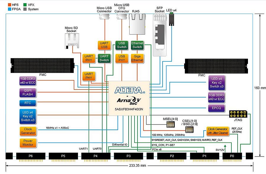
Figure 2-3 is the block diagram of the board. All the connections are established through the
Arria V SOC FPGA device to provide maximum flexibility for users.
Users can configure the
FPGA to implement any system design.

Figure 2-3 Block diagram of VPX-A5SoC
Detailed information about Figure 2-3 are listed below.
FPGA Device
- Arria V SOC 5ASXFB3H4F40I3N Device
- Dual-core ARM Cortex-A9 (HPS)
- 350K programmable logic elements
- 19,304 Kbits embedded memory
- 14 fractional PLLs
- 3 hard memory controllers
- 6.5336G transceivers
Configuration and Debug
- EPCQ for AS-Mode FPGA configure
- Configure through JTAG Interface(Blaster JTAG Heade,VPX JTAG Header)
Memory Device
- 1GB DDR3 SDRAM on FPGA
- 1GB DDR3 SDRAM on HPS
- Micro SD card socket on HPS
Communication
- USB 2.0 OTG (micro-AB USB connector)
- Two UART to USB (Normal Type-A USB connector)
- Giga Ethernet
Connectors
- Two FMC Connectors (support transceiver x8)
- 2x6 pin GPIO-Header (8 signal pins)
- SFP x1 connector
- One SFP connector
Switches, Buttons and Indicators
- 8 user Keys (FPGA x4, HPS x4)
- 8 user switches (FPGA x4, HPS x4)
- 12 user LEDs (FPGA x8, HPS x 4)
Power
- 12V DC input


