Word2wiki bal gsq

From Terasic Wiki

Jump to: navigation, search

=

Contents

Chpater1 Chapter 7PCI Express Design for Windows =

PCI Express is commonly used in consumer, server, and industrial applications, to link motherboard-mounted peripherals. From this demonstration, it will show how the PC Windows and FPGA communicate with each other through the PCI Express interface. Arria 10 Hard IP for PCI Express with Avalon-MM DMA IP is used in this demonstration. For detail about this IP, please refer to Altera document ug_a10_pcie_avmm_dma.pdf.


1-0-1 7.1 PCI Express System Infrastructure

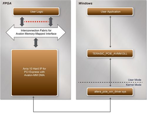
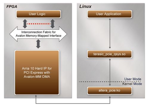
Figure 7-1 shows the infrastructure of the PCI Express System in this demonstration. It consists of two primary components: FPGA System and PC System. The FPGA System is developed based on Arria 10 Hard IP for PCI Express with Avalon-MM DMA. The application software on the PC side is developed by Terasic based on Altera’s PCIe kernel mode driver.

DE10-Advanced revC PCIE pic 1.jpg
Figure 7-1 Infrastructure of PCI Express System


1-0-2 7.2 PC PCI Express Software SDK

The FPGA System CD contains a PC Windows based SDK to allow users to develop their 64-bit software application on 64-bits Windows XP/7/10. The SDK is located in the "CDROM\Demonstrations\PCIe_SW_KIT\Windows" folder which includes:
* PCI Express Driver
  • PCI Express Library
  • PCI Express Examples


The kernel mode driver assumes the PCIe vendor ID (VID) is 0x1172 and the device ID (DID) is 0xE003. If different VID and DID are used in the design, users need to modify the PCIe vendor ID (VID) and device ID (DID) in the driver INF file accordingly.


The PCI Express Library is implemented as a single DLL named TERASIC_PCIE_AVMM.DLL.This file is a 64-bit DLL. With the DLL is exported to the software API, users can easily communicate with the FPGA. The library provides the following functions:
* Basic data read and write
  • Data read and write by DMA


For high performance data transmission, Altera AVMM DMA is required as the read and write operations are specified under the hardware design on the FPGA.


1-0-3 7.3 PCI Express Software Stack

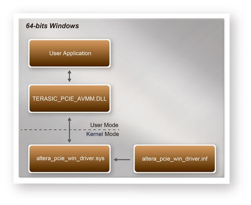
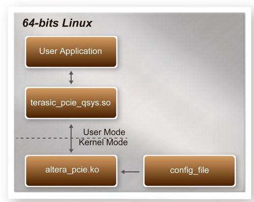
Figure 7-2 shows the software stack for the PCI Express application software on 64-bit Windows. The PCIe library module TERASIC_PCIE_AVMM.dll provides DMA and direct I/O access for user application program to communicate with FPGA. Users can develop their applications based on this DLL. The altera_pcie_win_driver.sys kernel driver is provided by Altera.

DE10-Advanced revC PCIE pic 2.jpg
Figure 7-2 PCI Express Software Stack
*
Install PCI Express Driver on Windows


The PCIe driver is locate in the folder:
"CDROM\Demonstrations\PCIe_SW_KIT\Windows\PCIe_Driver"
The folder includes the following four files:
* Altera_pcie_win_driver.cat
  • Altera_pcie_win_driver.inf
  • Altera_pcie_win_driver.sys
  • WdfCoinstaller01011.dll


To install the PCI Express driver, please execute the steps below:
# Make sure the DE10-Advanced and the PC are both powered off.
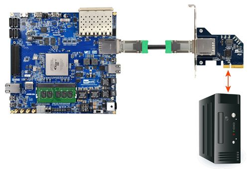
  1. Plug the PCIe adapter card into the PCIe slot on the PC motherboard. Use the PCIe cable to connect to the DE10-Advanced PCIE connector and the PCIe adapter card (See Figure 7-3)


DE10-Advanced revC PCIE pic 3.jpg
Figure 7-3 FPGA board connect to PC
# Power on your DE10-Advanced board and the host PC
  1. Make sure Altera Programmer and USB-Blaster II driver are installed
  2. Execute test.bat in "CDROM\Demonstrations\PCIe_Fundamental\demo_batch" to configure the FPGA
  3. Restart windows operation system
  4. Click Control Panel menu from Windows Start menu. Click Hardware and Sound item before clicking the Device Manager to launch the Device Manager dialog. There will be a PCI Device item in the dialog, as shown in Figure 7-4. Move the mouse cursor to the PCI Device item and right click it to select the Update Driver Software... item.


500px
Figure 7-4 Screenshot of launching Update Driver Software… dialog
# In the How do you want to search for driver software dialog, click Browse my computer for driver software item, as shown in Figure 7-5.


500px. Click the Next button.


500px, click the Install button.


500px. Click the Close button.


500px.


DE10-Advanced revC PCIE pic 9.jpg
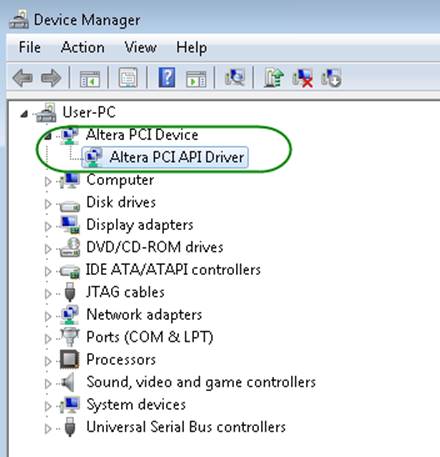
Figure 7-9 Altera PCI API Driver in Device Manager


  • Create a Software Application


All the files needed to create a PCIe software application are located in the directory CDROM\demonstration\PCIe_SW_KIT\Windows\PCIe_Library. It includes the following files:
* TERASIC_PCIE_AVMM.h
  • TERASIC_PCIE_AVMM.dll (64-bit dll)


Below lists the procedures to use the SDK files in users’ C/C++ project :
# Create a 64-bit C/C++ project.
  1. Include TERASIC_PCIE_AVMM.h in the C/C++ project.
  2. Copy TERASIC_PCIE_AVMM.dll to the folder where the project.exe is located.
  3. Dynamically load TERASIC_PCIE_AVMM.dll in C/C++ program. To load the dll, please refer to the PCIe fundamental example below.
  4. Call the SDK API to implement the desired application.


Users can easily communicate with the FPGA through the PCIe bus through the TERASIC_PCIE_AVMM.dll API. The details of API are described below:


1-0-4 7.4 PCI Express Library API

Below shows the exported API in the TERASIC_PCIE_AVMM.dll. The API prototype is defined in the TERASIC_PCIE_AVMM.h.
Note: the Linux library terasic_pcie_qsys.so also use the same API and header file.
*
PCIE_Open


Function:

Open a specified PCIe card with vendor ID, device ID, and matched card index.

Prototype:

PCIE_HANDLE PCIE_Open(

uint8_t wVendorID,

uint8_t wDeviceID,

uint8_t wCardIndex);

Parameters:

wVendorID:

Specify the desired vendor ID. A zero value means to ignore the vendor ID.

wDeviceID:

Specify the desired device ID. A zero value means to ignore the device ID.

wCardIndex:

Specify the matched card index, a zero based index, based on the matched vendor ID and device ID.

Return Value:

Return a handle to presents specified PCIe card. A positive value is return if the PCIe card is opened successfully. A value zero means failed to connect the target PCIe card.

This handle value is used as a parameter for other functions, e.g. PCIE_Read32.

Users need to call PCIE_Close to release handle once the handle is no more used.

* PCIE_Close


Function:

Close a handle associated to the PCIe card.

Prototype:

void PCIE_Close(

PCIE_HANDLE hPCIE);

Parameters:

hPCIE:

A PCIe handle return by PCIE_Open function.

Return Value:

None.

*
PCIE_Read32


Function:

Read a 32-bit data from the FPGA board.

Prototype:

bool PCIE_Read32(

PCIE_HANDLE hPCIE,

PCIE_BAR PcieBar,

PCIE_ADDRESS PcieAddress,

uint32_t *pdwData);

Parameters:

hPCIE:

A PCIe handle return by PCIE_Open function.

PcieBar:

Specify the target BAR.

PcieAddress:

Specify the target address in FPGA.

pdwData:

A buffer to retrieve the 32-bit data.

Return Value:

Return true if read data is successful; otherwise false is returned.

*
PCIE_Write32


Function:

Write a 32-bit data to the FPGA Board.

Prototype:

bool PCIE_Write32(

PCIE_HANDLE hPCIE,

PCIE_BAR PcieBar,

PCIE_ADDRESS PcieAddress,

uint32_t dwData);

Parameters:

hPCIE:

A PCIe handle return by PCIE_Open function.

PcieBar:

Specify the target BAR.

PcieAddress:

Specify the target address in FPGA.

dwData:

Specify a 32-bit data which will be written to FPGA board.

Return Value:

Return true if write data is successful; otherwise false is returned.

*
PCIE_Read8


Function:

Read an 8-bit data from the FPGA board.

Prototype:

bool PCIE_Read8(

PCIE_HANDLE hPCIE,

PCIE_BAR PcieBar,

PCIE_ADDRESS PcieAddress,

uint8_t *pByte);

Parameters:

hPCIE:

A PCIe handle return by PCIE_Open function.

PcieBar:

Specify the target BAR.

PcieAddress:

Specify the target address in FPGA.

pByte:

A buffer to retrieve the 8-bit data.

Return Value:

Return true if read data is successful; otherwise false is returned.

*
PCIE_Write8


Function:

Write an 8-bit data to the FPGA Board.

Prototype:

bool PCIE_Write8(

PCIE_HANDLE hPCIE,

PCIE_BAR PcieBar,

PCIE_ADDRESS PcieAddress,

uint8_t Byte);

Parameters:

hPCIE:

A PCIe handle return by PCIE_Open function.

PcieBar:

Specify the target BAR.

PcieAddress:

Specify the target address in FPGA.

Byte:

Specify an 8-bit data which will be written to FPGA board.

Return Value:

Return true if write data is successful; otherwise false is returned.

*
PCIE_DmaRead


Function:

Read data from the memory-mapped memory of FPGA board in DMA.

Maximal read size is (4GB-1) bytes.

Prototype:

bool PCIE_DmaRead(

PCIE_HANDLE hPCIE,

PCIE_LOCAL_ADDRESS LocalAddress,

void *pBuffer,

uint32_t dwBufSize

);

Parameters:

hPCIE:

A PCIe handle return by PCIE_Open function.

LocalAddress:

Specify the target memory-mapped address in FPGA.

pBuffer:

A pointer to a memory buffer to retrieved the data from FPGA. The size of buffer should be equal or larger the dwBufSize.

dwBufSize:

Specify the byte number of data retrieved from FPGA.

Return Value:

Return true if read data is successful; otherwise false is returned.

*
PCIE_DmaWrite


Function:

Write data to the memory-mapped memory of FPGA board in DMA.

Prototype:

bool PCIE_DmaWrite(

PCIE_HANDLE hPCIE,

PCIE_LOCAL_ADDRESS LocalAddress,

void *pData,

uint32_t dwDataSize

);

Parameters:

hPCIE:

A PCIe handle return by PCIE_Open function.

LocalAddress:

Specify the target memory mapped address in FPGA.

pData:

A pointer to a memory buffer to store the data which will be written to FPGA.

dwDataSize:

Specify the byte number of data which will be written to FPGA.

Return Value:

Return true if write data is successful; otherwise false is returned.

  • PCIE_ConfigRead32


Function:

Read PCIe Configuration Table. Read a 32-bit data by given a byte offset.

Prototype:

bool PCIE_ConfigRead32 (

PCIE_HANDLE hPCIE,

uint32_t Offset,

uint32_t *pdwData

);

Parameters:

hPCIE:

A PCIe handle return by PCIE_Open function.

Offset:

Specify the target byte of offset in PCIe configuration table.

pdwData:

A 4-bytes buffer to retrieve the 32-bit data.

Return Value:

Return true if read data is successful; otherwise false is returned.


1-0-5 7.5 PCIe Reference Design - Fundamental

The application reference design shows how to implement fundamental control and data transfer in DMA. In the design, basic I/O is used to control the BUTTON and LED on the FPGA board. High-speed data transfer is performed by DMA.
*
Demonstration Files Location


The demo file is located in the batch folder:
CDROM\Demonstrations\ PCIe_Fundamental\demo_batch
The folder includes following files:
* FPGA Configuration File: PCIe_Fundamental.sof
  • Download Batch file: test.bat
  • Windows Application Software folder : windows_app, includes
  • PCIE_FUNDAMENTAL.exe
  • TERASIC_PCIE_AVMM.DLL


*
Demonstration Setup
  1. Install the FPGA board on your PC as shown in Figure 7-3.
  2. Configure FPGA with PCIe_Fundamental.sof by executing the test.bat.
  3. Install PCIe driver if necessary. The driver is located in the folder:


CDROM\Demonstration\PCIe_SW_KIT\Windows\PCIe_Driver.
# Restart Windows
  1. Make sure the Windows has detected the FPGA Board by checking the Windows Control panel as shown in Figure 7-10.


Figure 7-10 Screenshot for PCIe Driver
# Goto windows_app folder, execute PCIE_FUNDAMENTAL.exe. A menu will appear as shown in Figure 7-11.


Figure 7-11 Screenshot of Program Menu
# Type 0 followed by a ENTER key to select Led Control item, then input 15 (hex 0x0f) will make all led on as shown in Figure 7-12. If input 0 (hex 0x00), all led will be turn off.


Figure 7-12 Screenshot of LED Control
# Type 1 followed by an ENTER key to select Button Status Read item. The button status will be report as shown in Figure 7-13.


Figure 7-13 Screenshot of Button Status Report
# Type 2 followed by an ENTER key to select DMA Testing item. The DMA test result will be report as shown in Figure 7-14.


DE10-Advanced revC PCIE pic 14.jpg
Figure 7-14 Screenshot of DMA Memory Test Result
# Type 99 followed by an ENTER key to exit this test program
  • Development Tools
  • Quartus Prime 18.0 Standard Edition
  • Visual C++ 2012
  • Demonstration Source Code Location
  • Quartus Project: Demonstrations\PCIe_Fundamental
  • C++ Project: Demonstrations\PCIe_SW_KIT\Windows\PCIE_FUNDAMENTAL


  • FPGA Application Design


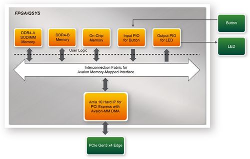
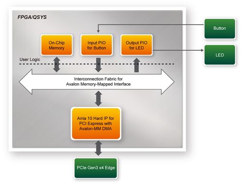
Figure 7-15 shows the system block diagram in the FPGA system. In the Qsys, Altera PIO controller is used to control the LED and monitor the Button Status, and the On-Chip memory is used for performing DMA testing. The PIO controllers and the On-Chip memory are connected to the PCI Express Hard IP controller through the Memory-Mapped Interface.

Figure 7-15 Hardware block diagram of the PCIe reference design
*
Windows Based Application Software Design


The application software project is built by Visual C++ 2012. The project includes the following major files:


Name Description
PCIE_FUNDAMENTAL.cpp Main program
PCIE.c Implement dynamically load for TERAISC_PCIE_AVMM.DLL
PCIE.h
TERASIC_PCIE_AVMM.h SDK library file, defines constant and data structure
The main program PCIE_FUNDAMENTAL.cpp includes the header file "PCIE.h" and defines the controller address according to the FPGA design.
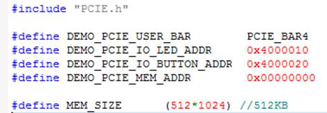
The base address of BUTTON and LED controllers are 0x4000010 and 0x4000020 based on PCIE_BAR4, in respectively. The on-chip memory base address is 0x00000000 relative to the DMA controller.


Before accessing the FPGA through PCI Express, the application first calls PCIE_Load to dynamically load the TERASIC_PCIE_AVMM.dll. Then, it call PCIE_Open to open the PCI Express driver. The constant DEFAULT_PCIE_VID and DEFAULT_PCIE_DID used in PCIE_Open are defined in TERASIC_PCIE_AVMM.h. If developer change the Vendor ID and Device ID and PCI Express IP, they also need to change the ID value define in TERASIC_PCIE_AVMM.h. If the return value of PCIE_Open is zero, it means the driver cannot be accessed successfully. In this case, please make sure:
* The FPGA is configured with the associated bit-stream file and the host is rebooted.
  • The PCI express driver is loaded successfully.

The LED control is implemented by calling PCIE_Write32 API, as shown below:


500px
The button status query is implemented by calling the PCIE_Read32 API, as shown below:


500px
The memory-mapped memory read and write test is implemented by PCIE_DmaWrite and PCIE_DmaRead API, as shown below:


1-0-6 7.6 PCIe Reference Design - DDR4

The application reference design shows how to add DDR4 Memory Controllers for DDR4-A SODIMM and on board DDR4-B into the PCIe Quartus project based on the PCIe_Fundamental Quartus project and perform 4GB data DMA for both SODIMM. Also, this demo shows how to call “PCIE_ConfigRead32” API to check PCIe link status.
*
Demonstration Files Location


The demo file is located in the batch folder:
CDROM\Demonstrations\PCIe_DDR4\demo_batch
The folder includes following files:
* FPGA Configuration File: PCIe_DDR4.sof
  • Download Batch file: test.bat
  • Windows Application Software folder : windows_app, includes
  • PCIE_DDR4.exe
  • TERASIC_PCIE_AVMM.dll


*
Demonstration Setup
  1. Install DDR4 2400 4GB SODIMM on the FPGA board.
  2. Install the FPGA board on your PC as shown in Figure 7-3.
  3. Configure FPGA with PCIe_DDR4.sof by executing the test.bat.
  4. Install PCIe driver if necessary.
  5. Restart Windows
  6. Make sure the Windows has detected the FPGA Board by checking the Windows Control panel.
  7. Goto windows_app folder, execute PCIE_DDR4.exe. A menu will appear as shown in Figure 7-16.


Figure 7-16 Screenshot of Program Menu
# Type 2 followed by a ENTER key to select Link Info item. The PCIe link information will be shown as in Figure 7-17. Gen3 link speed and x8 link width are expected.


Figure 7-17 Screenshot of Link Info
# Type 3 followed by an ENTER key to select DMA On-Chip Memory Test item. The DMA write and read test result will be report as shown in Figure 7-18.


Figure 7-18 Screenshot of On-Chip Memory DMA Test Result
# Type 4 followed by an ENTER key to select DMA DDR4-A SODIMM Memory Test item. The DMA write and read test result will be report as shown in Figure 7-19.


Figure 7-19 Screenshot of DDR4-A SOSIMM Memory DAM Test Result
# Type 5 followed by an ENTER key to select DMA DDR4-B Memory Test item. The DMA write and read test result will be report as shown in Figure 7-20.


Figure 7-20 Screenshot of DDR4-B SOSIMM Memory DAM Test Result
# Type 99 followed by an ENTER key to exit this test program.


*
Development Tools
  • Quartus Prime 18.0 Standard Edition
  • Visual C++ 2012
  • Demonstration Source Code Location
  • Quartus Project: Demonstrations\PCIE_DDR4
  • Visual C++ Project: Demonstrations\PCIe_SW_KIT\Windows\PCIe_DDR4


  • FPGA Application Design


Figure 7-21 shows the system block diagram in the FPGA system. In the Qsys, Altera PIO controller is used to control the LED and monitor the Button Status, and the On-Chip memory is used for performing DMA testing. The PIO controllers and the On-Chip memory are connected to the PCI Express Hard IP controller through the Memory-Mapped Interface.

DE10-Advanced revC PCIE pic 24.jpg
Figure 7-21 Hardware block diagram of the PCIe_DDR4 reference designWindows Based Application Software Design
The application software project is built by Visual C++ 2012. The project includes the following major files:


Name Description
PCIE_DDR4.cpp Main program
PCIE.c Implement dynamically load for TERAISC_PCIE_AVMM.DLL
PCIE.h
TERASIC_PCIE_AVMM.h SDK library file, defines constant and data structure
The main program PCIE_DDR4.cpp includes the header file "PCIE.h" and defines the controller address according to the FPGA design.


The base address of BUTTON and LED controllers are 0x4000010 and 0x4000020 based on PCIE_BAR4, in respectively. The on-chip memory base address is 0x00000000 relative to the DMA controller. The above definition is the same as those in PCIe Fundamental demo.


Before accessing the FPGA through PCI Express, the application first calls PCIE_Load to dynamically load the TERASIC_PCIE_AVMM.DLL. Then, it call PCIE_Open to open the PCI Express driver. The constant DEFAULT_PCIE_VID and DEFAULT_PCIE_DID used in PCIE_Open are defined in TERASIC_PCIE_AVMM.h. If developer change the Vendor ID and Device ID and PCI Express IP, they also need to change the ID value define in TERASIC_PCIE_AVMM.h. If the return value of PCIE_Open is zero, it means the driver cannot be accessed successfully. In this case, please make sure:
* The FPGA is configured with the associated bit-stream file and the host is rebooted.
  • The PCI express driver is loaded successfully.


The LED control is implemented by calling PCIE_Write32 API, as shown below:


500px


The button status query is implemented by calling the PCIE_Read32 API, as shown below:


500px
The memory-mapped memory read and write test is implemented by PCIE_DmaWrite and PCIE_DmaRead API, as shown below:

500px


The PCIe link information is implemented by PCIE_ConfigRead32 API, as shown below:


=

Chapter 8Chpater2 PCI Express Reference Design for Linux =

PCI Express is commonly used in consumer, server, and industrial applications, to link motherboard-mounted peripherals. From this demonstration, it will show how the PC Linux and FPGA communicate with each other through the PCI Express interface. Arria 10 Hard IP for PCI Express with Avalon-MM DMA IP is used in this demonstration. For detail about this IP, please refer to Altera document ug_a10_pcie_avmm_dma.pdf.


2-0-7 8.1 PCI Express System Infrastructure

Figure 8-1 shows the infrastructure of the PCI Express System in this demonstration. It consists of two primary components: FPGA System and PC System. The FPGA System is developed based on Arria 10 Hard IP for PCI Express with Avalon-MM DMA. The application software on the PC side is developed by Terasic based on Altera’s PCIe kernel mode driver.

Figure 8-1 Infrastructure of PCI Express System


2-0-8 8.2 PC PCI Express Software SDK

The FPGA System CD contains a PC Windows based SDK to allow users to develop their 64-bit software application on 64-bits Linux. CentOS 7.2 is recommended. The SDK is located in the “CDROM/Demonstrations/PCIe_SW_KIT/Linux” folder which includes:
* PCI Express Driver
  • PCI Express Library
  • PCI Express Examples


The kernel mode driver assumes the PCIe vendor ID (VID) is 0x1172 and the device ID (DID) is 0xE003. If different VID and DID are used in the design, users need to modify the PCIe vendor ID (VID) and device ID (DID) in the driver project and rebuild the driver. The ID is defined in the file PCIe_SW_KIT/Linux/PCIe_Driver/altera_pcie_cmd.h.


The PCI Express Library is implemented as a single .so file named terasic_pcie_qsys.so.This file is a 64-bit library file. With the library exported software API, users can easily communicate with the FPGA. The library provides the following functions:
* Basic data read and write
  • Data read and write by DMA


For high performance data transmission, Altera AVMM DMA is required as the read and write operations are specified under the hardware design on the FPGA.


2-0-9 8.3 PCI Express Software Stack

Figure 8-2 shows the software stack for the PCI Express application software on 64-bit Linux. The PCIe library module terasic_pcie_qys.so provides DMA and direct I/O access for user application program to communicate with FPGA. Users can develop their applications based on this .so library file. The altera_pcie.ko kernel driver is provided by Altera.

DE10-Advanced revC PCIE pic 30.jpg
Figure 8-2 PCI Express Software Stack
*
Install PCI Express Driver on Linux


To make sure the PCIe driver can meet your kernel of Linux distribution, the driver altera_pcie.ko should be recompile before use it. The PCIe driver project is locate in the folder:
"CDROM/Demonstrations/PCIe_SW_KIT/Linux/PCIe_Driver"

The folder includes the following files:* altera_pcie.c

  • altera_pcie.h
  • altera_pcie_cmd.h
  • Makefile
  • load_driver
  • unload
  • config_file


To compile and install the PCI Express driver, please execute the steps below:


  1. Make sure the DE10-Advanced and the PC are both powered off.
  2. Plug the PCIe adapter card into the PCIe slot on the PC motherboard. Use the PCIe cable to connect to the DE10-Advanced PCIE connector and the PCIe adapter card (See Figure 8-3)


DE10-Advanced revC PCIE pic 31.jpg
Figure 8-3 FPGA board connect to PC
# Power on your DE10-Advanced board and the host PC
  1. Open a terminal and use "cd" command to goto the folder"CDROM/Demonstrations/PCIe_Fundamental/demo_batch".
  2. Set QUARTUS_ROOTDIR variable pointing to the Quartus installation path. Set QUARTUS_ROOTDIR variable by tying the following commands in terminal. Replace “/home/centos/intelFPGA/18.0/quartus” to your quartus installation path.


export QUARTUS_ROOTDIR=/home/centos/intelFPGA/18.0/quartus
  1. Execute "sudo -E sh test.sh" command to configure the FPGA
  2. Restart Linux operation system. In Linux, open a terminal and use “cd” command to goto the PCIe_Driver folder
  3. Type the following commands to compile and install the driver altera_pcie.ko, and make sure driver is loaded successfully and FPGA is detected by the driver as shown in Figure 8-4.
  • make
  • sudo sh load_driver
  • dmesg | tail -n 15


DE10-Advanced revC PCIE pic 32.jpg

Figure 8-4 Screenshot of install PCIe driver
*
Create a Software Application


All the files needed to create a PCIe software application are located in the directory CDROM/Demonstrations/PCIe_SW_KIT/Linux/PCIe_Library. It includes the following files:
* TERASIC_PCIE_AVMM.h
  • terasic_pcie_qsys.so (64-bit library)


Below lists the procedures to use the library in users’ C/C++ project:
# Create a 64-bit C/C++ project.
  1. Include TERASIC_PCIE_AVMM.h in the C/C++ project.
  2. Copy terasic_pcie_qsys.so to the folder where the project execution file is located.
  3. Dynamically load terasic_pcie_qsys.so in C/C++ program. To load the terasic_pcie_qsys.so, please refer to the PCIe fundamental example below.
  4. Call the library API to implement the desired application.


Users can easily communicate with the FPGA through the PCIe bus through the terasic_pcie_qsys.so API. The details of API are described below:


2-0-10 8.4 PCI Express Library API

The API is the same as Windows Library. Please refer to the section 7.4 PCI Express Library API in this document.


2-0-11 8.5 PCIe Reference Design – Fundamental

The application reference design shows how to implement fundamental control and data transfer in DMA. In the design, basic I/O is used to control the BUTTON and LED on the FPGA board. High-speed data transfer is performed by DMA.
*
Demonstration Files Location


The demo file is located in the batch folder:
CDROM/Demonstrations/PCIe_Fundamental/demo_batch


The folder includes following files:
* FPGA Configuration File: PCIe_Fundamental.sof
  • Download Batch file: test.sh
  • Linux Application Software folder : linux_app, includes
  • PCIE_FUNDAMENTAL
  • terasic_pcie_qsys.so
  • Demonstration Setup
  1. Install the FPGA board on your PC as shown in Figure8-3.
  2. Open a terminal and use "cd" command to goto "CDROM/Demonstrations/PCIe_Fundamental/demo_batch".
  3. Set QUARTUS_ROOTDIR variable pointing to the Quartus installation path. Set QUARTUS_ROOTDIR variable by tying the following commands in terminal. Replace /home/centos/intelFPGA/18.0/quartus to your quartus installation path.


export QUARTUS_ROOTDIR=/home/centos/intelFPGA/18.0/quartus
  1. Execute "sudo -E sh test.sh" command to configure the FPGA
  2. Restart Linux
  3. Install PCIe driver. The driver is located in the folder:


CDROM/Demonstration/PCIe_SW_KIT/Linux/PCIe_Driver.
# Type “ls –l /dev/altera_pcie*” to make sure the Linux has detected the FPGA Board. If the FPGA board is detected, developers can find the /dev/altera_pcieX(where X is 0~255) in Linux file system as shown below.


500px.


500px

Figure 8-5 Screenshot of Program Menu
# Type 0 followed by a ENTER key to select Led Control item, then input 3 (hex 0x03) will make all led on as shown in Figure 8-6. If input 0 (hex 0x00), all led will be turn off.


500px

Figure 8-6 Screenshot of LED Control
#
Type 1 followed by an ENTER key to select Button Status Read item. The button status will be report as shown in Figure 8-7.


Figure 8-7 Screenshot of Button Status Report
#
Type 2 followed by an ENTER key to select DMA Testing item. The DMA test result will be report as shown in Figure 8-8.


Figure 8-8 Screenshot of DMA Memory Test Result
# Type 99 followed by an ENTER key to exit this test program
  • Development Tools
  • Quartus Prime 18.0 Standard Edition
  • GNU Compiler Collection, Version 4.8 is recommend
  • Demonstration Source Code Location
  • Quartus Project: Demonstrations/PCIe_Fundamental
  • C++ Project: Demonstrations/PCIe_SW_KIT/Linux/PCIE_FUNDAMENTAL
  • FPGA Application Design


Figure 8-9 shows the system block diagram in the FPGA system. In the Qsys, Altera PIO controller is used to control the LED and monitor the Button Status, and the On-Chip memory is used for performing DMA testing. The PIO controllers and the On-Chip memory are connected to the PCI Express Hard IP controller through the Memory-Mapped Interface.

Figure 8-9 Hardware block diagram of the PCIe reference design
*
Linux Based Application Software DesignThe application software project is built by GNU Toolchain. The project includes the following major files:


Name Description
PCIE_FUNDAMENTAL.cpp Main program
PCIE.c Implement dynamically load for terasic_pcie_qsys.so library file
PCIE.h
TERASIC_PCIE_AVMM.h SDK library file, defines constant and data structure
The main program PCIE_FUNDAMENTAL.cpp includes the header file "PCIE.h" and defines the controller address according to the FPGA design.
DE10-Advanced revC PCIE pic 39.jpg
The base address of BUTTON and LED controllers are 0x4000010 and 0x4000020 based on PCIE_BAR4, in respectively. The on-chip memory base address is 0x00000000 relative to the DMA controller.


Before accessing the FPGA through PCI Express, the application first calls PCIE_Load to dynamically load the terasic_pcie_qsys.so. Then, it call PCIE_Open to open the PCI Express driver. The constant DEFAULT_PCIE_VID and DEFAULT_PCIE_DID used in PCIE_Open are defined in TERASIC_PCIE_AVMM.h. If developer change the Vendor ID and Device ID and PCI Express IP, they also need to change the ID value define in TERASIC_PCIE_AVMM.h. If the return value of PCIE_Open is zero, it means the driver cannot be accessed successfully. In this case, please make sure:
* The FPGA is configured with the associated bit-stream file and the host is rebooted.
  • The PCI express driver is loaded successfully.


The LED control is implemented by calling PCIE_Write32 API, as shown below:


DE10-Advanced revC PCIE pic 40.jpg
The button status query is implemented by calling the PCIE_Read32 API, as shown below:


DE10-Advanced revC PCIE pic 41.jpg
The memory-mapped memory read and write test is implemented by PCIE_DmaWrite and PCIE_DmaRead API, as shown below:


2-0-12 8.5 PCIe Reference Design - DDR4

The application reference design shows how to add DDR4 Memory Controllers for DDR4-A SODIMM and on board DDR4-B into the PCIe Quartus project based on the PCIe_Fundamental Quartus project and perform 4GB data DMA for both SODIMM. Also, this demo shows how to call “PCIE_ConfigRead32” API to check PCIe link status.
*
Demonstration Files Location


The demo file is located in the batch folder:
CDROM/Demonstrations/ PCIe_DDR4/demo_batch
The folder includes following files:
* FPGA Configuration File: PCIe_DDR4sof
  • Download Batch file: test.sh
  • Linux Application Software folder : linux_app, includes
  • PCIE_DDR4
  • terasic_pcie_qsys.so
  • Demonstration Setup
  1. Install DDR4 2400 4GB SODIMM on the FPGA board.
  2. Install the FPGA board on your PC as shown in Figure8-3.
  3. Open a terminal and use "cd" command to goto "CDROM/Demonstrations/PCIe_Fundamental/demo_batch".
  4. Set QUARTUS_ROOTDIR variable pointing to the Quartus installation path. Set QUARTUS_ROOTDIR variable by tying the following commands in terminal. Replace /home/centos/intelFPGA/18.0/quartus to your quartus installation path.


export QUARTUS_ROOTDIR=/home/centos/intelFPGA/18.0/quartus
  1. Execute "sudo -E sh test.sh" command to configure the FPGA
  2. Restart Linux
  3. Install PCIe driver.
  4. Make sure the Linux has detected the FPGA Board.
  5. Goto linux_app folder, execute PCIE_DDR4. A menu will appear as shown in Figure 8-10.


DE10-Advanced revC PCIE pic 42.jpg

Figure 8-10 Screenshot of Program Menu
# Type 2 followed by an ENTER key to select Link Info item. The PCIe link information will be shown as in Figure 8-11. Gen3 link speed and x8 link width are expected.


500px

Figure 8-11 Screenshot of Link Info
#
Type 3 followed by an ENTER key to select DMA On-Chip Memory Test item. The DMA write and read test result will be report as shown in Figure 8-12.


Figure 8-12 Screenshot of On-Chip Memory DMA Test Result
# Type 4 followed by an ENTER key to select DMA DDR4-A SODIMM Memory Test item. The DMA write and read test result will be report as shown in Figure 8-14.


500px

Figure 8-14 Screenshot of DDR4-A SOSIMM Memory DAM Test Result
# Type 5 followed by an ENTER key to select DMA DDR4-B Memory Test item. The DMA write and read test result will be report as shown in Figure 8-15.


500px

Figure 8-15 Screenshot of DDR4-B SOSIMM Memory DAM Test Result
# Type 99 followed by an ENTER key to exit this test program.


  • Development Tools
  • Quartus Prime 18.0 Standard Edition
  • GNU Compiler Collection, Version 4.8 is recommended
  • Demonstration Source Code Location
  • Quartus Project: Demonstrations/PCIE_DDR4
  • C++ Project: Demonstrations/PCIe_SW_KIT/Linux/PCIe_DDR4


  • FPGA Application Design


Figure 8-16 shows the system block diagram in the FPGA system. In the Qsys, Altera PIO controller is used to control the LED and monitor the Button Status, and the On-Chip memory is used for performing DMA testing. The PIO controllers and the On-Chip memory are connected to the PCI Express Hard IP controller through the Memory-Mapped Interface.
Figure 8-16 Hardware block diagram of the PCIe_DDR4 reference design
*
Linux Based Application Software Design


The application software project is built by GNU Toolchain. The project includes the following major files:


Name Description
PCIE_DDR4.cpp Main program
PCIE.c Implement dynamically load for terasic_pcie_qsys.so library file
PCIE.h
TERASIC_PCIE_AVMM.h SDK library file, defines constant and data structure
The main program PCIE_DDR4.cpp includes the header file "PCIE.h" and defines the controller address according to the FPGA design.
DE10-Advanced revC PCIE pic 48.jpg
The base address of BUTTON and LED controllers are 0x4000010 and 0x4000020 based on PCIE_BAR4, in respectively. The on-chip memory base address is 0x00000000 relative to the DMA controller. The above definition is the same as those in PCIe Fundamental demo.


Before accessing the FPGA through PCI Express, the application first calls PCIE_Load to dynamically load the terasic_pcie_qsys.so. Then, it call PCIE_Open to open the PCI Express driver. The constant DEFAULT_PCIE_VID and DEFAULT_PCIE_DID used in PCIE_Open are defined in TERASIC_PCIE_AVMM.h. If developer change the Vendor ID and Device ID and PCI Express IP, they also need to change the ID value define in TERASIC_PCIE_AVMM.h. If the return value of PCIE_Open is zero, it means the driver cannot be accessed successfully. In this case, please make sure:
* The FPGA is configured with the associated bit-stream file and the host is rebooted.
  • The PCI express driver is loaded successfully.


The LED control is implemented by calling PCIE_Write32 API, as shown below:


500px
The button status query is implemented by calling the PCIE_Read32 API, as shown below:


DE10-Advanced revC PCIE pic 50.jpg
The memory-mapped memory read and write test is implemented by PCIE_DmaWrite and PCIE_DmaRead API, as shown below:

500px


The PCIe link information is implemented by PCIE_ConfigRead32 API, as shown below:
Personal tools