DE10-Advance usermanual revB
From Terasic Wiki
(→4.3 SFP+ Connector) |
(→4.4 SATA) |
||
| Line 137: | Line 137: | ||
==4.4 SATA== | ==4.4 SATA== | ||
| + | Four Serial ATA (SATA) ports are available on the FPGA development board which are computer bus standard with a primary function of transferring data between the motherboard and mass storage devices (such as hard drives, optical drives, and solid-state disks). Supporting a storage interface is just one of many different applications an FPGA can be used in storage appliances. The Arria 10 SoC device can bridge different protocols such as bridging simple bus I/Os like PCI Express (PCIe) to SATA or network interfaces such as Gigabit Ethernet (GbE) to SATA. The SATA interface supports SATA 3.0 standard with connection speed of 6 Gbps based on Arria 10 SoC device with integrated transceivers compliant to SATA electrical standards.<br/> | ||
| + | The four Serial ATA (SATA) ports include two available ports for device and two available ports for host capable of implementing SATA solution with a design that consists of both host and target(device side) functions.Figure 4-4 depicts the host and device design examples.<br/> | ||
| + | ::::[[File:SATA.jpg|600px]]<br/> | ||
| + | :::::::Figure 4-4 PC and storage device connection to the Arria 10 SoC FPGA<br/> | ||
| + | The transmitter and receiver signals of the SATA ports are connected directly to the Arria 10 SoC transceiver channels to provide SATA IO connectivity to both host and target devices. To verify the functionality of the SATA host/device ports, a connection can be established between the two ports by using a SATA cable as Figure 4-5 depicts the associated signals connected.Table 4-7 lists the SATA pin assignments, signal names and functions.<br/> | ||
| + | :::[[File:SATA1.jpg|600px]]<br/> | ||
| + | ::::::::Figure 4-5 Pin connection between SATA connectors<br/> | ||
| + | :::::Table 4-7 SATA Pin Assignments,Signal Names and Functions<br/> | ||
| + | :{| class="wikitable" | ||
| + | |- | ||
| + | !Signal Name!!FPGA Pin Number!!Description!!I/O Standard | ||
| + | |- | ||
| + | |colspan="4" |Device | ||
| + | |- | ||
| + | |SATA_DEVICE_REFCLK_p || PIN_M31 || SATA Device reference clock ||LVDS | ||
| + | |- | ||
| + | | SATA_DEVICE_REFCLK_n || PIN_M30 || SATA Device reference clock ||LVDS | ||
| + | |- | ||
| + | | SATA_DEVICE_RX_n0 || PIN_D34 ||Differential receive data input after DC blocking capacitor ||HSSI DIFFERENTIAL I/O | ||
| + | |- | ||
| + | | SATA_DEVICE_RX_n1 ||PIN_B34 ||Differential receive data input after DC blocking capacitor ||HSSI DIFFERENTIAL I/O | ||
| + | |- | ||
| + | | SATA_DEVICE_TX_n0 || PIN_B38 || Differential transmit data output before DC blocking capacitor ||HSSI DIFFERENTIAL I/O | ||
| + | |- | ||
| + | | SATA_DEVICE_TX_n1 ||PIN_A36 || Differential transmit data output before DC blocking capacitor ||HSSI DIFFERENTIAL I/O | ||
| + | |- | ||
| + | |SATA_DEVICE_TX_p0||PIN_B39||Differential transmit data output before DC blocking capacitor||HSSI DIFFERENTIAL I/O | ||
| + | |- | ||
| + | |SATA_DEVICE_TX_p1||PIN_A37||Differential transmit data output before DC blocking capacitor||HSSI DIFFERENTIAL I/O | ||
| + | |- | ||
| + | |SATA_DEVICE_RX_p0||PIN_D35||Differential receive data input after DC blocking capacitor||HSSI DIFFERENTIAL I/O | ||
| + | |- | ||
| + | |SATA_DEVICE_RX_p1||PIN_B35||Differential receive data input after DC blocking capacitor||HSSI DIFFERENTIAL I/O | ||
| + | |- | ||
| + | |colspan="4" |Host | ||
| + | |- | ||
| + | |SATA_HOST_REFCLK_p||PIN_AF31||SATA Host reference clock||LVDS | ||
| + | |- | ||
| + | |SATA_HOST_REFCLK_n||PIN_AF30||SATA Host reference clock||LVDS | ||
| + | |- | ||
| + | |SATA_HOST_TX_p0||PIN_AJ37||Differential transmit data output before DC blocking capacitor||HSSI DIFFERENTIAL I/O | ||
| + | |- | ||
| + | |SATA_HOST_TX_p1||PIN_AH39||Differential transmit data output before DC blocking capacitor||HSSI DIFFERENTIAL I/O | ||
| + | |- | ||
| + | |SATA_HOST_RX_p0||PIN_AE33||Differential receive data input after DC blocking capacitor||HSSI DIFFERENTIAL I/O | ||
| + | |- | ||
| + | |SATA_HOST_RX_p1||PIN_AF35||Differential receive data input after DC blocking capacitor||HSSI DIFFERENTIAL I/O | ||
| + | |- | ||
| + | |SATA_HOST_TX_n0||PIN_AJ36||Differential transmit data output before DC blocking capacitor||HSSI DIFFERENTIAL I/O | ||
| + | |- | ||
| + | |SATA_HOST_TX_n1||PIN_AH38||Differential transmit data output before DC blocking capacitor||HSSI DIFFERENTIAL I/O | ||
| + | |- | ||
| + | |SATA_HOST_RX_n0||PIN_AE32||Differential receive data input after DC blocking capacitor||HSSI DIFFERENTIAL I/O | ||
| + | |- | ||
| + | |SATA_HOST_RX_n1||PIN_AF34||Differential receive data input after DC blocking capacitor||HSSI DIFFERENTIAL I/O | ||
| + | |} | ||
| + | |||
==4.5 PCIe== | ==4.5 PCIe== | ||
==<span style="color:#ff0000;">4.6 DDR4</span>== | ==<span style="color:#ff0000;">4.6 DDR4</span>== | ||
Revision as of 09:30, 25 June 2018
Chapter 1 DE10-Advanced Development Kit
1.1 Package Contents
1.2 DE10-Advanced System CD
1.3 Getting Help
Chapter 2 Introduction of the DE10-Advanced Board
2.1 Layout and Components
2.2 Block Diagram of the DE10-Advanced Board
3 Chapter 3 Board Setting and Status component
3.1 Board Setting Switches
3.1.1 USB Type C Connector Setting Switches
3.1.2 Mode Select Switches
3.2 Board Setting Headers
3.2.1 JTAG Interface Header
3.2.2 FMC_VCCIO Select Header
3.2.3 DDR4 VCCIO Select Header
3.2.4 External USB Blaster Header
3.3 Status LED
3.3.1 System MAX
3.3.2 UART Interface
3.3.3 SFP Interface
3.3.4 Ethernet Interface
3.3.5 Power
3.4 JTAG Interface
Chapter 4 FPGA Fabric component
4.1 USB Type C Port
4.2 Display Port
4.3 SFP+ Connector
The development board has four independent 10G SFP+ connectors that use one transceiver channel each from the Arria 10 SoC FPGA device. These modules take in serial data from the Arria 10 SoC FPGA device and transform them to optical signals. The board includes cage assemblies for the SFP+ connectors.Figure 4-3 shows the connections between the SFP+ and Arria 10 SoC FPGA.
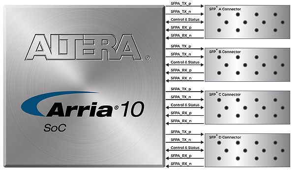
- Figure 4-3 Connection between the SFP+ and Arria 10 SoC FPGA
- Figure 4-3 Connection between the SFP+ and Arria 10 SoC FPGA

Table 4-3, Table 4-4, Table 4-5 and Table 4-6 list the four QSF+ connectors assignments and signal names relative to the Arria 10 SoC FPGA
- Table 4-3 SFP+ A Pin Assignments, Signal Names and Functions
Signal Name FPGA Pin Number Description I/O Standard SFPA_TXDISABLE PIN_AR28 Turns off and disables the transmitter output 1.2V SFPA_TXFAULT PIN_AP28 Transmitter fault 1.2V SFPA_TX_p PIN_AG37 Transmiter data HSSI DIFFERENTIAL I/O SFPA_RX_p PIN_AD35 Receiver data HSSI DIFFERENTIAL I/O SFPA_LOS PIN_AN6 Signal loss indicator 1.2V SFPA_MOD0_PRSNT_n PIN_AU4 Module present 1.2V SFPA_RATESEL0 PIN_AM19 Rate select 0 3.3V SFPA_RATESEL1 PIN_AN17 Rate select 1 3.3V SFPA_TX_n PIN_AG36 Transmitter data HSSI DIFFERENTIAL I/O SFPA_RX_n PIN_AD34 Receiver data HSSI DIFFERENTIAL I/O
- Table 4-4 SFP+ B Pin Assignments, Signal Names and Functions
Signal Name FPGA Pin Number Description I/O Standard SFPB_TXDISABLE PIN_AU5 Turns off and disables the transmitter output 1.2V SFPB_TXFAULT PIN_AE10 Transmitter fault 1.2V SFPB_TX_p PIN_AF39 Transmiter data HSSI DIFFERENTIAL I/O SFPB_RX_p PIN_AC37 Receiver data HSSI DIFFERENTIAL I/O SFPB_LOS PIN_AN12 Signal loss indicator 1.2V SFPB_MOD0_PRSNT_n PIN_AT5 Module present 1.2V SFPB_RATESEL0 PIN_AR18 Rate select 0 3.3V SFPB_RATESEL1 PIN_AP18 Rate select 1 3.3V SFPB_TX_n PIN_AF38 Transmitter data HSSI DIFFERENTIAL I/O SFPB_RX_n PIN_AC36 Receiver data HSSI DIFFERENTIAL I/O
- Table 4-5 SFP+ C Pin Assignments, Signal Names and Functions
Signal Name FPGA Pin Number Description I/O Standard SFPC_TXDISABLE PIN_AP30 Turns off and disables the transmitter output 1.2V SFPC_TXFAULT PIN_AP28 Transmitter fault 1.2V SFPC_TX_p PIN_AE37 Transmiter data HSSI DIFFERENTIAL I/O SFPC_RX_p PIN_AC33 Receiver data HSSI DIFFERENTIAL I/O SFPC_LOS PIN_AN28 Signal loss indicator 1.2V SFPC_MOD0_PRSNT_n PIN_B27 Module present 1.2V SFPC_RATESEL0 PIN_AK18 Rate select 0 3.3V SFPC_RATESEL1 PIN_AR17 Rate select 1 3.3V SFPC_TX_n PIN_AE36 Transmitter data HSSI DIFFERENTIAL I/O SFPC_RX_n PIN_AC32 Receiver data HSSI DIFFERENTIAL I/O
- Table 4-6 SFP+ D Pin Assignments, Signal Names and Functions
Signal Name FPGA Pin Number Description I/O Standard SFPD_TXDISABLE PIN_AR28 Turns off and disables the transmitter output 1.2V SFPD_TXFAULT PIN_AP21 Transmitter fault 1.2V SFPD_TX_p PIN_AD39 Transmiter data HSSI DIFFERENTIAL I/O SFPD_RX_p PIN_AB35 Receiver data HSSI DIFFERENTIAL I/O SFPD_LOS PIN_D26 Signal loss indicator 1.2V SFPD_MOD0_PRSNT_n PIN_AL28 Module present 1.2V SFPD_RATESEL0 PIN_AH18 Rate select 0 3.3V SFPD_RATESEL1 PIN_AW19 Rate select 1 3.3V SFPD_TX_n PIN_AD38 Transmitter data HSSI DIFFERENTIAL I/O SFPD_RX_n PIN_AB34 Receiver data HSSI DIFFERENTIAL I/O
4.4 SATA
Four Serial ATA (SATA) ports are available on the FPGA development board which are computer bus standard with a primary function of transferring data between the motherboard and mass storage devices (such as hard drives, optical drives, and solid-state disks). Supporting a storage interface is just one of many different applications an FPGA can be used in storage appliances. The Arria 10 SoC device can bridge different protocols such as bridging simple bus I/Os like PCI Express (PCIe) to SATA or network interfaces such as Gigabit Ethernet (GbE) to SATA. The SATA interface supports SATA 3.0 standard with connection speed of 6 Gbps based on Arria 10 SoC device with integrated transceivers compliant to SATA electrical standards.
The four Serial ATA (SATA) ports include two available ports for device and two available ports for host capable of implementing SATA solution with a design that consists of both host and target(device side) functions.Figure 4-4 depicts the host and device design examples.
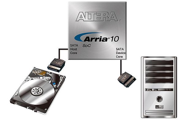
- Figure 4-4 PC and storage device connection to the Arria 10 SoC FPGA
- Figure 4-4 PC and storage device connection to the Arria 10 SoC FPGA

The transmitter and receiver signals of the SATA ports are connected directly to the Arria 10 SoC transceiver channels to provide SATA IO connectivity to both host and target devices. To verify the functionality of the SATA host/device ports, a connection can be established between the two ports by using a SATA cable as Figure 4-5 depicts the associated signals connected.Table 4-7 lists the SATA pin assignments, signal names and functions.
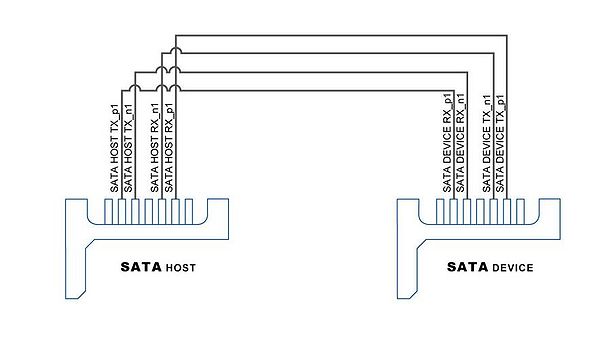
- Figure 4-5 Pin connection between SATA connectors
- Figure 4-5 Pin connection between SATA connectors
- Table 4-7 SATA Pin Assignments,Signal Names and Functions

Signal Name FPGA Pin Number Description I/O Standard Device SATA_DEVICE_REFCLK_p PIN_M31 SATA Device reference clock LVDS SATA_DEVICE_REFCLK_n PIN_M30 SATA Device reference clock LVDS SATA_DEVICE_RX_n0 PIN_D34 Differential receive data input after DC blocking capacitor HSSI DIFFERENTIAL I/O SATA_DEVICE_RX_n1 PIN_B34 Differential receive data input after DC blocking capacitor HSSI DIFFERENTIAL I/O SATA_DEVICE_TX_n0 PIN_B38 Differential transmit data output before DC blocking capacitor HSSI DIFFERENTIAL I/O SATA_DEVICE_TX_n1 PIN_A36 Differential transmit data output before DC blocking capacitor HSSI DIFFERENTIAL I/O SATA_DEVICE_TX_p0 PIN_B39 Differential transmit data output before DC blocking capacitor HSSI DIFFERENTIAL I/O SATA_DEVICE_TX_p1 PIN_A37 Differential transmit data output before DC blocking capacitor HSSI DIFFERENTIAL I/O SATA_DEVICE_RX_p0 PIN_D35 Differential receive data input after DC blocking capacitor HSSI DIFFERENTIAL I/O SATA_DEVICE_RX_p1 PIN_B35 Differential receive data input after DC blocking capacitor HSSI DIFFERENTIAL I/O Host SATA_HOST_REFCLK_p PIN_AF31 SATA Host reference clock LVDS SATA_HOST_REFCLK_n PIN_AF30 SATA Host reference clock LVDS SATA_HOST_TX_p0 PIN_AJ37 Differential transmit data output before DC blocking capacitor HSSI DIFFERENTIAL I/O SATA_HOST_TX_p1 PIN_AH39 Differential transmit data output before DC blocking capacitor HSSI DIFFERENTIAL I/O SATA_HOST_RX_p0 PIN_AE33 Differential receive data input after DC blocking capacitor HSSI DIFFERENTIAL I/O SATA_HOST_RX_p1 PIN_AF35 Differential receive data input after DC blocking capacitor HSSI DIFFERENTIAL I/O SATA_HOST_TX_n0 PIN_AJ36 Differential transmit data output before DC blocking capacitor HSSI DIFFERENTIAL I/O SATA_HOST_TX_n1 PIN_AH38 Differential transmit data output before DC blocking capacitor HSSI DIFFERENTIAL I/O SATA_HOST_RX_n0 PIN_AE32 Differential receive data input after DC blocking capacitor HSSI DIFFERENTIAL I/O SATA_HOST_RX_n1 PIN_AF34 Differential receive data input after DC blocking capacitor HSSI DIFFERENTIAL I/O