DE10-Advanced revC demo: PCIe Reference Design - DDR4
From Terasic Wiki
(→FPGA Application Design) |
(→FPGA Application Design) |
||
| Line 62: | Line 62: | ||
The application software project is built by Visual C++ 2012. The project includes the following major files: | The application software project is built by Visual C++ 2012. The project includes the following major files: | ||
| - | + | ||
:{| class="wikitable" | :{| class="wikitable" | ||
|- | |- | ||
| Line 78: | Line 78: | ||
||SDK library file, defines constant and data structure | ||SDK library file, defines constant and data structure | ||
|} | |} | ||
| - | |||
| + | The main program PCIE_DDR4.cpp includes the header file "PCIE.h" and defines the controller address according to the FPGA design. | ||
| - | |||
| - | + | [[Image: DE10-Advanced_revC_PCIE_pic_25.png|600px]] | |
| + | |||
| + | The base address of BUTTON and LED controllers are 0x4000010 and 0x4000020 based on PCIE_BAR4, in respectively. The on-chip memory base address is 0x00000000 relative to the DMA controller. | ||
| + | <span style="color:#ff0000;">The above definition is the same as those in PCIe Fundamental demo.</span> | ||
| Line 101: | Line 103: | ||
| - | + | The button status query is implemented by calling the '''PCIE_Read32''' API, as shown below: | |
| - | + | [[Image: DE10-Advanced_revC_PCIE_pic_27.jpg|500px]] | |
| - | + | ||
| - | + | ||
| - | + | ||
| - | + | ||
<div style="color:#404040;"></div> | <div style="color:#404040;"></div> | ||
Revision as of 18:21, 27 August 2018
Contents |
Demonstration Files Location
The demo file is located in the batch folder: CDROM\Demonstrations\PCIe_DDR4\demo_batch
The folder includes following files:</div>* FPGA Configuration File: PCIe_DDR4.sof
- Download Batch file: test.bat
- Windows Application Software folder : windows_app, includes
- PCIE_DDR4.exe
- TERASIC_PCIE_AVMM.dll
Demonstration Setup
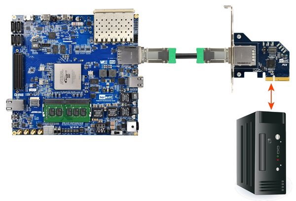
- Install DDR4 2400 4GB SODIMM on the FPGA board.
- Install the FPGA board on your PC as shown in Figure 1-1.
-
- Figure 1-1 FPGA board connect to PC
- Configure FPGA with PCIe_DDR4.sof by executing the test.bat.
- Install PCIe driver if necessary.
- Restart Windows
- Make sure the Windows has detected the FPGA Board by checking the Windows Control panel.
- Goto windows_app folder, execute PCIE_DDR4.exe. A menu will appear as shown in Figure 1-2.
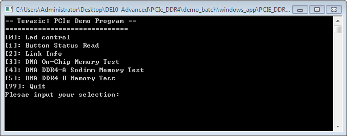
- Figure 1-2 Screenshot of Program Menu</div>
- Type 2 followed by a ENTER key to select Link Info item. The PCIe link information will be shown as in Figure 1-3. Gen3 link speed and x8 link width are expected.
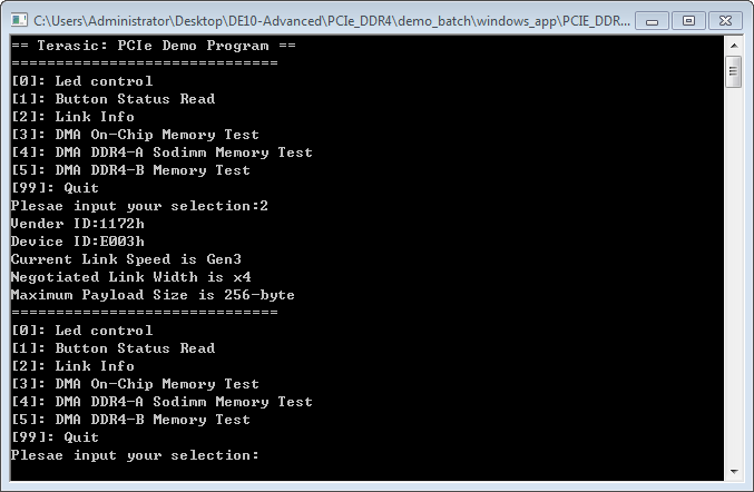
- Figure 1-3 Screenshot of Link Info
- Type 3 followed by an ENTER key to select DMA On-Chip Memory Test item. The DMA write and read test result will be report as shown in Figure 1-4.
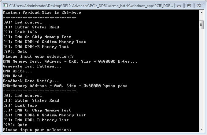
- Figure 1-4 Screenshot of On-Chip Memory DMA Test Result
- Type 4 followed by an ENTER key to select DMA DDR4-A SODIMM Memory Test item. The DMA write and read test result will be report as shown in Figure 1-5.
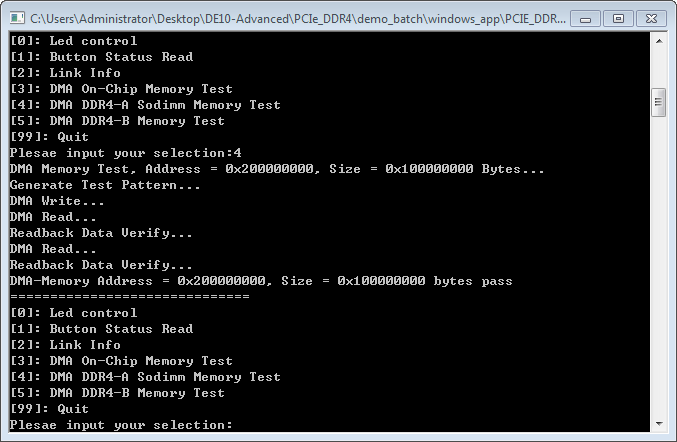
- Figure 1-5 Screenshot of DDR4-A SOSIMM Memory DAM Test Result
- Type 5 followed by an ENTER key to select DMA DDR4-B Memory Test item. The DMA write and read test result will be report as shown in Figure 1-6.
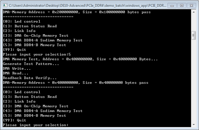
- Figure 1-6 Screenshot of DDR4-B SOSIMM Memory DAM Test Result
- Type 99 followed by an ENTER key to exit this test program.


Development Tools
- Quartus Prime 18.0 Standard Edition
- Visual C++ 2012
Demonstration Source Code Location
- Quartus Project: Demonstrations\PCIE_DDR4
- Visual C++ Project: Demonstrations\PCIe_SW_KIT\Windows\PCIe_DDR4
FPGA Application Design
Figure 1-7 shows the system block diagram in the FPGA system. In the Qsys, Altera PIO controller is used to control the LED and monitor the Button Status, and the On-Chip memory is used for performing DMA testing. The PIO controllers and the On-Chip memory are connected to the PCI Express Hard IP controller through the Memory-Mapped Interface.

Figure 1-7 Hardware block diagram of the PCIe_DDR4 reference designWindows Based Application Software Design
The application software project is built by Visual C++ 2012. The project includes the following major files:
NAME Description PCIE_FUNDAMENTAL.cpp Main program PCIE.c Implement dynamically load for TERAISC_PCIE_AVMM.DLL PCIE.h TERASIC_PCIE_AVMM.h SDK library file, defines constant and data structure
The main program PCIE_DDR4.cpp includes the header file "PCIE.h" and defines the controller address according to the FPGA design.

The base address of BUTTON and LED controllers are 0x4000010 and 0x4000020 based on PCIE_BAR4, in respectively. The on-chip memory base address is 0x00000000 relative to the DMA controller. The above definition is the same as those in PCIe Fundamental demo.
- The PCI express driver is loaded successfully.
| 500px |
The button status query is implemented by calling the PCIE_Read32 API, as shown below:
The PCIe link information is implemented by PCIE_ConfigRead32 API, as shown below: