DE10-Advanced revC demo: PCIe Reference Design - DDR4
From Terasic Wiki
Contents |
Demonstration Files Location
The demo file is located in the batch folder: CDROM\Demonstrations\PCIe_DDR4\demo_batch
The folder includes following files:</div>* FPGA Configuration File: PCIe_DDR4.sof
- Download Batch file: test.bat
- Windows Application Software folder : windows_app, includes
- PCIE_DDR4.exe
- TERASIC_PCIE_AVMM.dll
Demonstration Setup
- Install DDR4 2400 4GB SODIMM on the FPGA board.
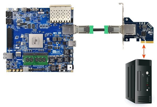
- Install the FPGA board on your PC as shown in Figure 1-1.
-
- Figure 1-1 FPGA board connect to PC
- Configure FPGA with PCIe_DDR4.sof by executing the test.bat.
- Install PCIe driver if necessary.
- Restart Windows
- Make sure the Windows has detected the FPGA Board by checking the Windows Control panel.
- Goto windows_app folder, execute PCIE_DDR4.exe. A menu will appear as shown in Figure 1-2.
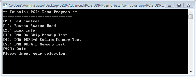
- Figure 1-2 Screenshot of Program Menu</div>
- Type 2 followed by a ENTER key to select Link Info item. The PCIe link information will be shown as in Figure 1-3. Gen3 link speed and x8 link width are expected.
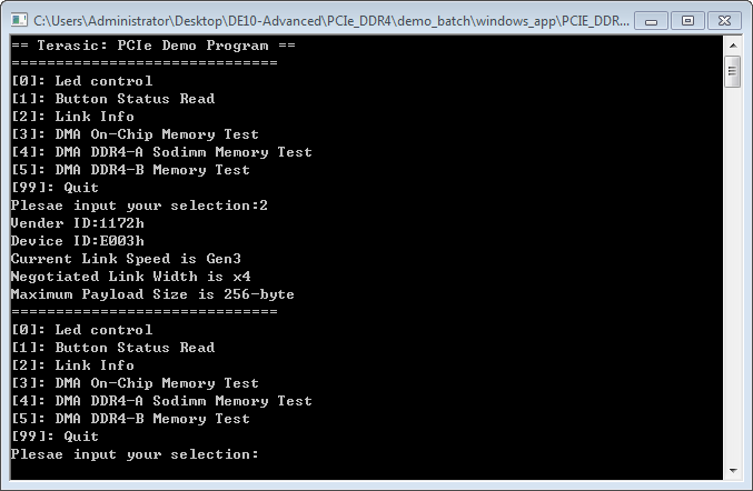
- Figure 1-3 Screenshot of Link Info
- Type 3 followed by an ENTER key to select DMA On-Chip Memory Test item. The DMA write and read test result will be report as shown in Figure 1-4.
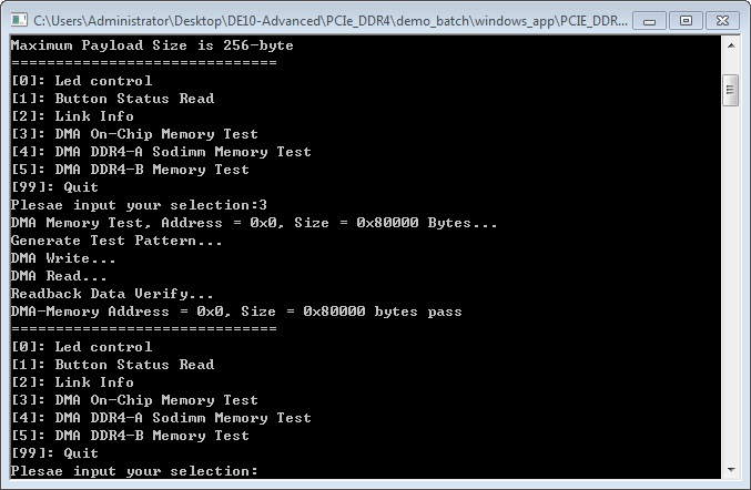
- Figure 1-4 Screenshot of On-Chip Memory DMA Test Result
- Type 4 followed by an ENTER key to select DMA DDR4-A SODIMM Memory Test item. The DMA write and read test result will be report as shown in Figure 1-5.
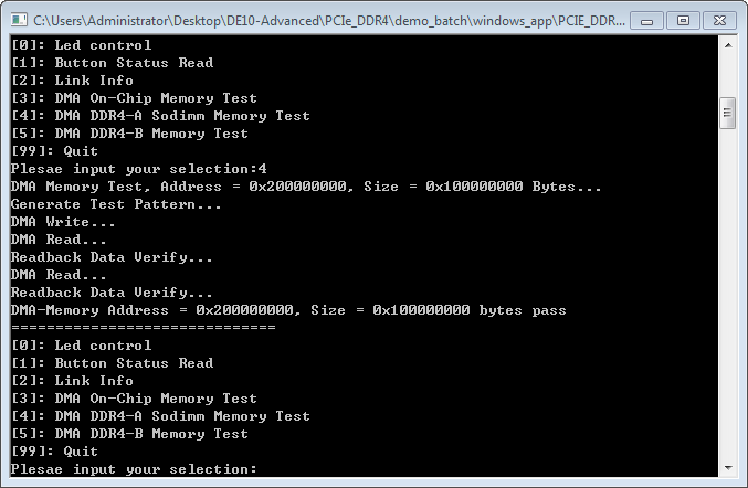
- Figure 1-5 Screenshot of DDR4-A SOSIMM Memory DAM Test Result
- Type 5 followed by an ENTER key to select DMA DDR4-B Memory Test item. The DMA write and read test result will be report as shown in Figure 1-6.
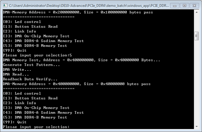
- Figure 1-6 Screenshot of DDR4-B SOSIMM Memory DAM Test Result
- Type 99 followed by an ENTER key to exit this test program.


Development Tools
- Quartus Prime 18.0 Standard Edition
- Visual C++ 2012
Demonstration Source Code Location
- Quartus Project: Demonstrations\PCIE_DDR4
- Visual C++ Project: Demonstrations\PCIe_SW_KIT\Windows\PCIe_DDR4
FPGA Application Design
Figure 1-7 shows the system block diagram in the FPGA system. In the Qsys, Altera PIO controller is used to control the LED and monitor the Button Status, and the On-Chip memory is used for performing DMA testing. The PIO controllers and the On-Chip memory are connected to the PCI Express Hard IP controller through the Memory-Mapped Interface.

Figure 1-7 Hardware block diagram of the PCIe_DDR4 reference designWindows Based Application Software Design
The application software project is built by Visual C++ 2012. The project includes the following major files:
- Table 1-1 LED Indicators
NAME Description PCIE_FUNDAMENTAL.cpp Main program PCIE.c Implement dynamically load for TERAISC_PCIE_AVMM.DLL PCIE.h TERASIC_PCIE_AVMM.h SDK library file, defines constant and data structure
- The PCI express driver is loaded successfully.
| 500px |
| 500px |
The PCIe link information is implemented by PCIE_ConfigRead32 API, as shown below: