F2G User Manual
From Terasic Wiki
Contents |
Chpater1 Introduction
The F2G board is designed to convert a FPGA Mezzanine Card(FMC) or FPGA Mezzanine Card Plus(FMC+) interface to four 2x20pin expansion prototype(GPIO) connectors, which are compatible with the expansion headers of the Terasic DE-Series board(Such as DE2-115/DE10-Standard). Users can connect up to four GPIO connectors onto a FMC-interfaced host board via a F2G board.
1-1 Kit Contents
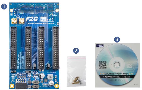
Figure 1-1 shows a photograph of the F2G package.
- F2G Card
- Screw & Copper Pillar Pakage
- CD Download Guide
1-2 Features
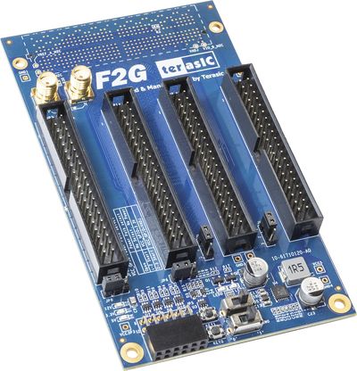
Figure 1-2 shows the photo of a F2G board. The important functions of the F2G are listed below:
- FMC High-Pin Count Interface.
- IO standard is dependent on FMC Voltage of the Mother board.
- Four 2x20 GPIO Headers.
- 2x6 TMD Header.
- SMA Clock Input.
- Button x2.
- SWtich x2.
- LED x2.
1-3 Layout and Components
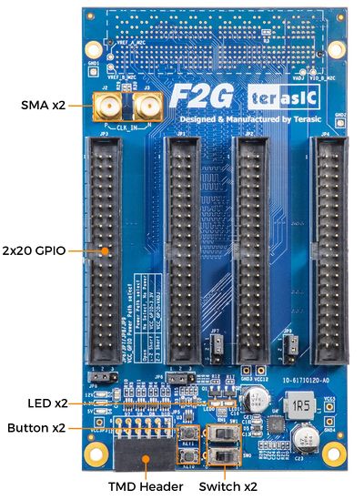
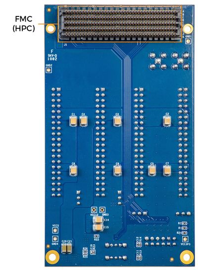
This section presents the features and design characteristics of the board. A photograph of the board is shown in Figure 1-3 and Figure 1-4 It depicts the layout of the board and indicates the location of the connectors and key components.
1-4 Block Diagram
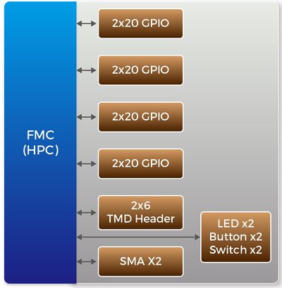
Figure 1-5 gives the block diagram of the board. According to the FMC Vita 57 specification, the FMC connector can be divided into two specifications by I/O pin numbers: high pin count and low pin count. Therefore, in the figure, we list 3 groups I/O pin in the FMC connector such as LA, HA and HB. Pins with a L prefix (LA) shall have connector contacts populated in the low-pin and high-pin count connectors Pins with a H prefix (HA and HB) shall have connector contacts populated only in the high-pin count connector. This will allow users to understand which F2G board interfaces can be used for their FPGA motherboard.
1-5 Mechanical Specifications
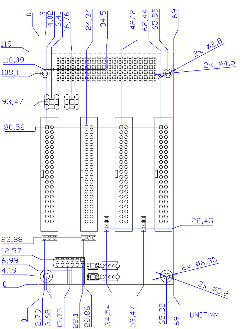
Figure 1-6 is the Mechanical Layout of F2G board.
1-6 Getting Help
Contact us via the following methods for further technical assistance:
- Terasic Inc.9F, No.176, Sec.2, Gongdao 5th Rd, East Dist, Hsinchu City, Taiwan 300-70
- Email : support@terasic.com
- Web : www.terasic.com
