HERO Doucment Hardware Manual English
From Terasic Wiki
Chapter 1
Chapter 2
Chapter 3
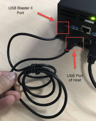
Connect the USB Blaster II port to the Host computer USB port by using a mini usb cable.
Figure 3-3 Connect USB Blaster II Port to CPU Host
In the HERO platform, since the user can work with the OpenCL or OpenVNIO toolkit to configure the FPGA through the PCIe interface, there is a less time to use the USB Blaster II interface for the configuration.
The following are the main situations to use the USB blaster II port:
1. Replace or Update the flash configuration file in the FPGA accelerator, it needs to program the Flash via the USB Blaster II port.
2. If the user wants to design by himself and running the FPGA accelerator without any other toolkits, the configuration file can be downloaded into the FPGA device through the USB Blaster II port to complete the FPGA configuration as the normal FPGA board works.
3. When the version of the programmed OpenCL configuration file in Flash is different from the version of the .aocx file running, it cannot support to configure FPGA through PCIe direclty. It needs to downloaded through USB Blaster to run the FPGA in the desired state.
3.4 DDR4 Memory
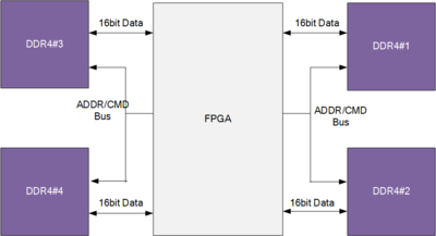
The FPGA accelerator provides four DDR4 devices with a total capacity of 2GB (see figure 2-x). They can be used for data caching. The available bit width is up to 64bit and runs at 2400Mhz(FPGA speed grade: I1). The maximum bandwidth is 153.6Gbps theoretically. The I/O pin assignment of DDR4 is shown in table 2-x.
Figure 3-4 DDR4 to FPGA connection
3.5 PCIe interface
There is a PCIe Gen 3 x4 interface on the FPGA accelerator which can be used to connect to the CPU host system. Working with the built-in transceiver and integrated PCI Express hardcore IP module on the Arria 10 GX device, it can provide a fully integrated PCI Express compatibility solution.
In the HERO platform, with the assistance of OpenCL or OpenVINO toolkit, the CPU host system can configure the FPGA to complete the acceleration logic through the PCIe interface, and transmit and retrieve various data about computing the acceleration.
3.6 USB 3.0 Host
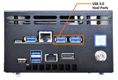
The FPGA accelerator retains A USB 3.0-compatible xHCI Host controller (TI :TUSB7320IRKM) to equip with two USB 3.0 Standard-A interfaces. Which is expected that the FPGA accelerator can provide two USB 3.0 Host. Note, this is a reserved function, unable to use it currently.
The interface between the TUSB7320IRKM controller and FPGA follows the PCIe x1 Gen2 protocol. So a pair of TX/RX transceiver should be used to connect these two devices. Please refer to the tusb7320.pdf document in the CD\Datasheet folder for the detailed information.
Figure 3-5 USB Blaster II Port of the FPGA Accelerator
3.7 USB 3.0 Device
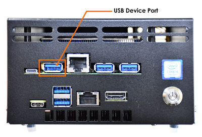
The FPGA accelerator is equipped with a USB3.0 controller which is the Cypress model CYUSB3014. It can be used as the USB3.0 Device and related applications of USB2.0 OTG. The user can use this port to transmit data from the FPGA to the CPU system or other hosts.
See more details from the CD\Datasheet\FX3 subfolder.
Figure 3-6 USB Blaster II Port of the FPGA Accelerator
3.8 Gigabit Ethernet
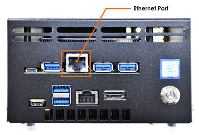
The FPGA accelerator board is configured with a 10/100/1000 gigabit Ethernet transceiver chip MARVELL88E1111.The chip is an auto-negotiated Ethernet PHY that connects to the FPGA using the default SGMII MAC interface.The transmission takes the form of LVDS I/O with a speed of 1.2Gbps. Users can place a MAC IP in the FPGA to work this accelerator communicating with external devices via Ethernet.
Figure 3-7 Ethernet Port of the FPGA Board
3.9 Clock Circuit
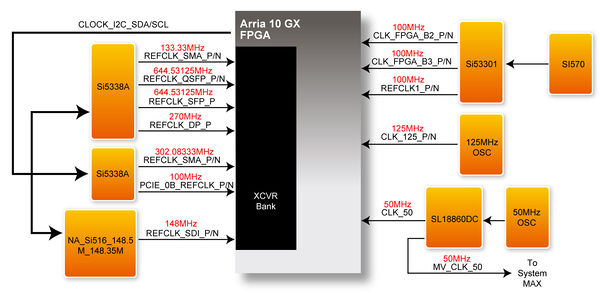
As shown in figure x, there is a variety of clock frequencies (OSC & on board PLL) for a variety of FPGA applications. The output frequency of PLL which is provided to FPGA transceiver bank can be changed through I2C interface for the different requirements. And the other input of fixed frequency is also being connected into the FPGA clock input dedicated pin. User can also get the frequency multiplied or frequency divided by using the FPGA internal PLL megafunction.
Figure 3-8 Clock Networks
