Bill Nace
- Associate Teaching Professor
- Department of Electrical and Computer Engineering
- Carnegie Mellon University
- 2015 Spira Award for Excellence in Teaching
- Awarded by Lutron Electronics Co., Inc.
Teaches
- Design of Digital Systems (UG core class)
- Logic Design and Verification (UG depth class)
- Advanced Digital Design (UG capstone design class)
- plus Networking / Distributed Systems courses
- Design of Digital Systems (UG core class)
- Awarded by Lutron Electronics Co., Inc.
 Intro
Intro
Altera has introduced a SoC variation for the beloved Cyclone V chip, and now Terasic provides a board that lets you try it out. The DE10-Standard
is a fairly nice learning platform for those interested in SoC development. A such, it fleshes out Terasic's line of educational boards, while also providing power for engineering development and prototyping tasks.
Why you should trust me
I have been teaching undergraduate classes about digital design on FPGAs since 2002. For the past 9 years, I've taught those courses at Carnegie Mellon University, a top-tier school in the field of Computer Engineering. I teach three separate courses on digital design: an introductory course, an advanced course in digital logic verification and a capstone design course, all of which use various FPGAs. As I cast my eyes around my office, I count 8 different FPGA boards; four of which are from Terasic. My experience is hands-on — I'm not the sort of professor to hand a board to a Teaching Assistant without spending some time playing with it myself.
For this review, I spent about 35 hours experimenting with the DE10-Standard
, reading manuals, configuring FPGA hardware through custom SystemVerilog, and experimenting with Terasic's SoC examples.
Opening the Box
|
|
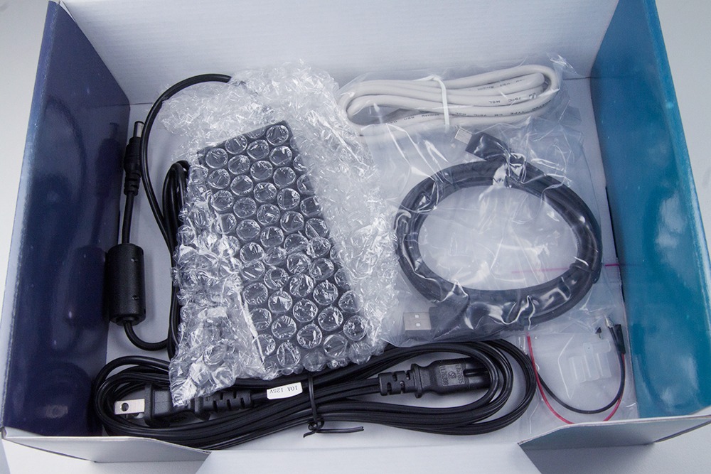
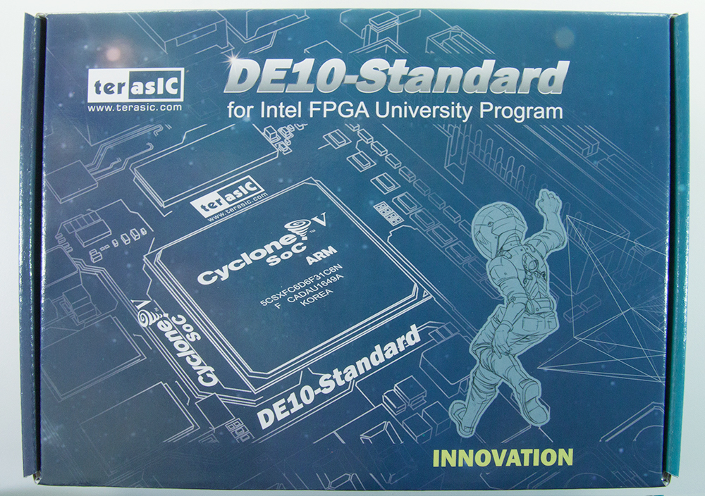
Like every Terasic board I've ever received, it comes in a blue box with nice foam padding. The box includes the board, a power supply and power cord, two USB cables and some marketing materials. One of the USB cables is the USB-blaster cord (USB-A to USB-B), while the other is a USB-A to Mini-B used for communicating with the ARM CPU.
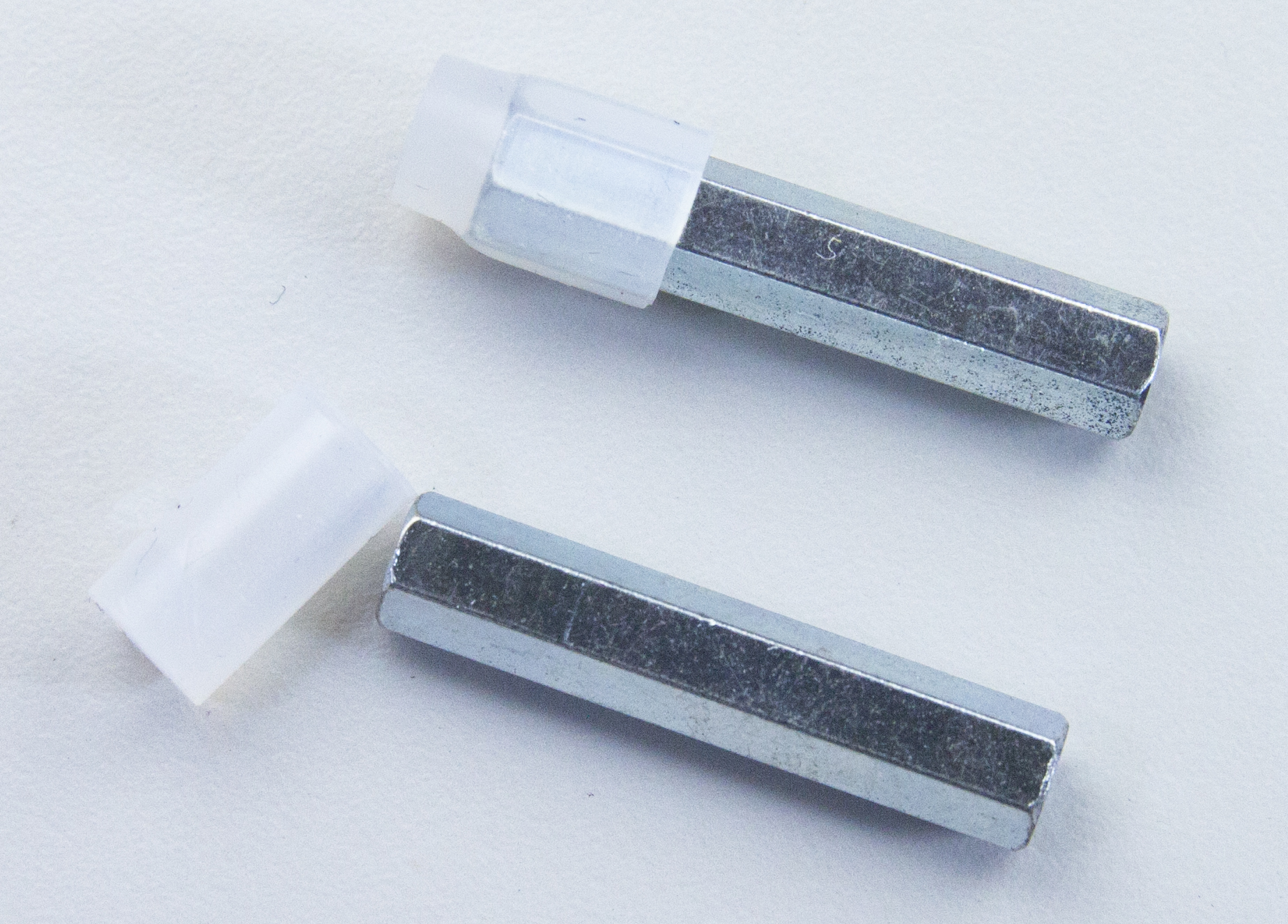
My board didn't come with the little rubber foot covers that I've gotten used to on other Terasic boards. A quick glance at the Quick Start Guide shows they are supposed to be included, so perhaps this was simply an oversight and your board will include them. Certainly not a deal breaker.
Of course, one of the first things anyone does with a new FPGA board is to take a tour and try to identify the components. This board is nicely outfitted with plenty of peripherals and connectors.
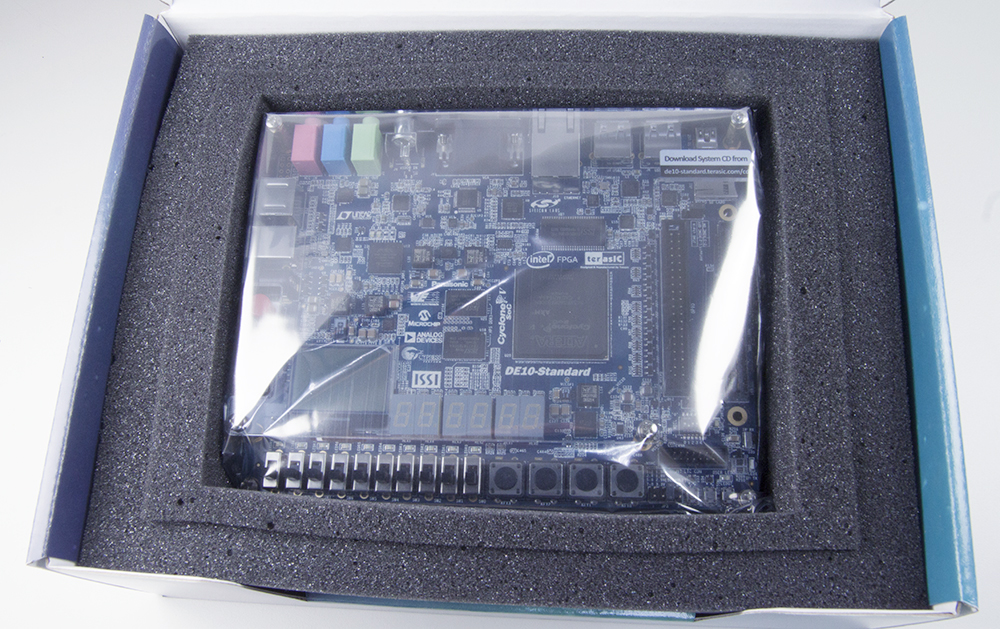
|
The centerpiece is, of course, the Cyclone V SoC chip. It still bears the Altera mark, though silkscreening on the board has been updated since Intel purchased Altera. Let's get a bit of potential confusion out of the way first. Even though Terasic's board is named the DE10-Standard
, the device is not one of Altera's new Cyclone 10 series (nor do the new DE10-Nano
and DE10-Lite
boards have such devices). Rather the device is a Cyclone V 5CSXFC6D6F31C6N. A few minutes with the Altera FPGA family tables makes me think that it is an SX variant with 110K logic elements (LE), about 5.5 Mbits of block RAM, 112 DSP blocks and 224 multipliers.
Being an SoC chip means having a processor on the same silicon as the FPGA fabric. In the case of the DE10-Standard, the processor is a dual-core ARM Cortex-A9, clocked at 925 MHz. Nice!
Continuing the tour of board, let's take a look at the peripherals. There are plenty of connectors for lots of different types of wires: Gigabit Ethernet, an RCA jack (for TV signal input in NTSC, PAL or SECAM format), audio connectors (with the same 24-bit audio CODEC as we've seen on the DE2-115 board), and a PS/2 connector for keyboard or mouse. I avoided USB in that list, as there are a total of 4 USB connectors that I wanted to discuss separately.

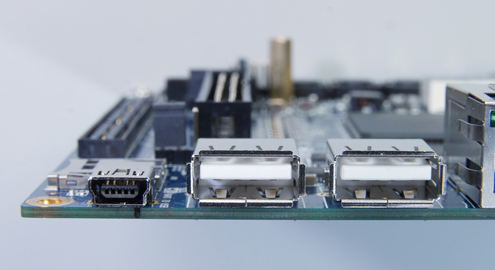
One is the USB-B connector for USB-Blaster configuration of the board. Two Type-A connectors and a Mini-B connector are also available, though they all connect to the ARM processor, not the FPGA fabric. The idea is that you can connect a USB keyboard and mouse to the Type-As and use the Mini-B connector for a communications channel to a console.
In several different places, the manuals refer to an HDMI monitor connector, but that is an error — the monitor connection is a VGA, connected to a DAC with 8-bits of color in each of the three channels.
I was glad to see a fair amount of simple I/O: 10 switches, 10 LEDs, four pushbuttons and six 7-Segment diplays. I'd like to see even more (the 18 switches, 26 LEDs, and eight 7-Segment displays of the DE2-115 board have spoiled me), but even this amount far exceeds the count from other manufacturer's boards. As I teach introductory digital logic classes, it is essential to have plenty of simple I/O for easing students into the idea of controlling lots of hardware.

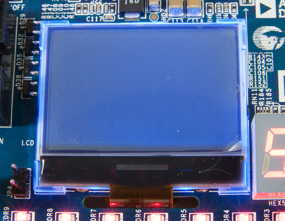 There are even more peripherals on the board: accelerometer, IR receiver/transmitter pair, eight channel ADC, SDRAM, configuration device, Micro SD card socket and a sweet-looking LCD screen. They should keep me entertained as I experiment with them over the coming months. If the board is missing your favorite peripheral, there is also some expansion capability; a 40-pin GPIO ("General Purpose I/O") expansion header and an HSMC connector.
This last, a "High-Speed Mezzanine Card," is a standard interface used to allow connections to daughter-cards. Such cards are available for a variety of digital and analog hardware from a variety of vendors, including Terasic.
I mentioned earlier that the USB connectors were hooked up to the CPU, not the FPGA fabric, and I need to explain the ramifications. You see, the silicon of the Cyclone V-SoC chip contains FPGA fabric and the ARM CPU, each on it's own partition. The CPU partition is often referred to as HPS or "Hard Processor System." In this context, the "Hard" CPU is built into the silicon as opposed to a "Soft" CPU (like NIOS) where the FPGA fabric is configured to implement a CPU. The pins on the chip are connected, within the silicon, to one or the other partition -- not both. So a particular pin is usable for I/O from the partition it is connected to: either the FPGA fabric or the HPS. Terasic engineers, when designing the board, had to choose which peripherals were more likely to be used from which partition, as the connections are permanent and not configurable. Their choices seem to be reasonable, though I had been looking forward to a fabric-connected USB connector for a project in my advanced course. Of course, access to the fabric-connected peripherals is possible from software running on the CPU, because the there are access pathways to allow the CPU and fabric partitions to intercommunicate. Getting hardware access to a HPS peripheral isn't possible, however. So, my dreams of having students build finite-state machines to drive the LCD display won't be realized on this board.
My First FPGA
As my heart is in digital design, I first started to mess around with the FPGA fabric and the fabric-connected peripherals. Terasic's "Learning Roadmap" makes the same suggestion -- get comfortable with FPGA before HPS.
So, I plugged in the DE10-Standard
board. The provided power supply is a 3.5A, pretty beefy. It also is not a plug-blocking wall wart, for which I am grateful. It is a small-ish in-line brick with detachable power cable. Yes, I'm reviewing a power supply, which might seem a bit obsessive. However, I'm grateful for Terasic's choices, as we've had trouble with power supplies for other boards in the confined cable runs of my undergraduate lab.
I fired up Quartus Prime, version 16.1 (the most recent version as of this writing), and put together a simple combinational circuitry project to test the board, the configuration process, and the assertion levels of the simple I/O. Synthesis completed without error, which was pretty amazing.
I ran into a few toolchain issues when trying to configure the device. None turned out to be show-stoppers, but the driver-installation and Quartus programming interactions never seem to go as smoothly as the manuals would lead you to believe. Most of those problems are Quartus' fault, so I won't count them against the DE10-Standard board. However, this is the first time I've seen the programmer ask for which JTAG ID the FPGA matches, with eight different choices. I'm not sure what's going on here, but the Terasic manual tells you which selection to make (5CSXFC6D6), so I was able to configure the FPGA chip. My curiosity wants to understand what the choices mean and why they exist, but the manual doesn't help with that.
A few seconds later, the programmer reported success. For the most part, the I/O works as you'd expect. A minor complaint is that the manual claims the KEY push-buttons are active high, when they are actually active-low (i.e. push them to get a zero). I didn't experiment with everything on the FPGA partition yet, but the basic I/O, the seven-segment displays, and the VGA work as advertised.
SOC
Using a SoC is a much more complex task than just programming the FPGA fabric. The issue is that there are lots of new interfaces to learn, some of which require new tools in an already complex toolchain. The Cyclone V experience is no different from other vendor's SoC implementations, though Terasic has done quite a bit to try to ease the learning shock.
For instance, Terasic provides a Linux image that has already been customized to the ARM-9 CPU on the chip. This image, if copied to an SD Card, is used to boot the CPU. As long as you are intending to use Linux, this is a great help. However, if you want bare-metal access to the CPU, you are going to have to figure that one out on your own. I've had students do it (on other boards and other chips), so it is possible. Just one more level of complexity, though.
Since you are going to want to use the CPU to access peripherals, you are going to have to understand how to do so from the Linux environment. There are some libraries included to access some of the peripherals. Yet another layer (or two) of complexity.
Terasic provides example C-language programs to help get you started. There is the "Hello, World" program that shows UART console use. An LCD demo lets you see text and graphics drawn on the LCD screen. Other demos show how to use the GPIO connector and another how to access the accelerometer.
The explanations behind some of the demonstrations are pretty sparse, however. Most of the code has very minimal commenting; and in some cases, like the I2C demo, the comments are only partially written. Learning how the libraries work and what the parameters are will require lots of experimenting. There isn't any sort of "reference manual" that allows you to lookup the access mechanisms for whatever hardware interface you desire.
The demonstrations do go very far beyond a simple "Hello, World" which is much to Terasic's credit. One shows how to use a Bluetooth USB dongle to communicate to an app. Another shows how to use a network connection (via Ethernet) to communicate with an NTP time server. This last is significantly aided by using curl rather than straight socket programming, but is still a nice demo.
A final category of demonstration teaches how to get the CPU in the HPS partition to work with components built into the FPGA fabric partition. These are significantly complex demonstrations and it would be nice to have better documentation describing why the designs need to be constructed as they are. But, again, it is to Terasic's credit that such demonstrations exist at all. At least one has something to start with, to experiment with, to begin the learning
process.
Judgment
SoC development is clearly going to be a significant player in engineering of hardware systems. All major FPGA vendors are investing in SoC capabilities and producing interesting chips. Clearly, the academic world needs to figure out how to teach these capabilities. Engineers in the field will need to do some on-the-job training to build their SoC skills.
Terasic has anticipated those desires and responded by creating the DE10-Standard
board. This board has plenty of capability to prototype a wide range of SoC systems. The simple I/O will be incredibly useful for those just starting out, but the complex devices and expansion capability of HSMC daughter boards will satisfy those with deeper needs.
I think the DE10-Standard
board is well-positioned to serve this wide-ranging constituency. It compares favorably with boards from other vendors and is priced competitively. Those in academia will be pleased with the Academic discount as well. This is exactly the sort of board that should be used as the centerpiece of a textbook on SoC development. I know I would enjoy reading such a text.
In conclusion, I find that I have two thumbs extended in the "up" position on this board. There is a lot to love about the DE10-Standard
and very few complaints.
(By Bill Nace, Associate Teaching Professor at Carnegie Mellon University,
Apr 23, 2017
)

