DE10 Advance revC demo: GHRD Project
From Terasic Wiki
The term GHRD is short for Golden Hardware Reference Design. The GRD project provide by Terasic for the DE10-Advanced development board is located in the CD folder: CD-ROM\Demonstration\SOC_FPGA\ de10_advanced_ghrd.
The project consists of the following components:
- ARM Cortex™-A9 MPCore HPS
- Two user push-button inputs
- Two user DIP switch inputs
- Two user I/O for LED outputs
- 256 KB of on-chip memory
- JTAG to Avalon master bridges
- Interrupt capturer for use with System Console
- System ID
The memory map of system peripherals in the FPGA portion of the SoC as viewed by the MPU starts at the lightweight HPS-to-FPGA base address 0xFF20_0000. The MPU can access these peripherals through the Address offset setting in the Qsys. User can open the GHRD project with Quartus Software. Then open the de10_advanced_ghrd.qsys file with the Qsys tool. Figure 4-2 lists the address map of the peripherals which are connected to the lightweight HPS-to-FPGA.
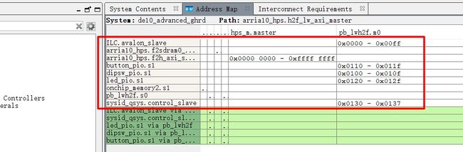
- Figure 4-2 FPGA peripherals address map

All the Avalon Conduit signals of these peripherals are connected to the I/O pins of the SoCFPGA on DE10-Advanced board as shown in the Figure 4-3.
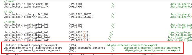
- Figure 4-3 Connection in the top design
